Cirrus Logic CS5550 User Manual
Cs5550 two-channel, low-cost a/d converter, Features, Description
Copyright
© Cirrus Logic, Inc. 2005
(All Rights Reserved)
CS5550
Two-channel, Low-cost A/D Converter
Features
z
Power Consumption <12 mW
- with VD+ = 3.3 V
z
Adjustable Input Range on AIN1
±
z
GND-referenced Signals with Single Supply
z
On-chip 2.5 V Reference (25 ppm/°C typ)
z
Simple Three-wire Digital Serial Interface
z
Power Supply Configurations
VA+ = +5 V; AGND = 0 V; VD+ = +3.3 V to +5 V
Description
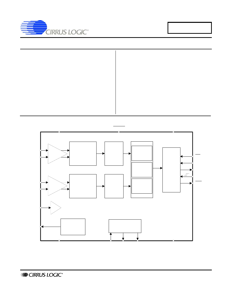
The CS5550 combines two
∆Σ ADCs and a serial
interface on a single chip. The CS5550 has
on-chip functionality to facilitate offset and gain
calibration. The CS5550 features a bi-directional
serial interface for communication with a
microcontroller.
ORDERING INFORMATION:
CS5550-IS
-40
°C to +85°C
24-pin SSOP
CS5550-ISZ
-40
°C to +85°C, Lead-free 24-pin SSOP
VA+
VD+
VREFIN
VREFOUT
AGND
XIN
XOUT CPUCLK
DGND
CS
SDO
SDI
SCLK
INT
Voltage
Reference
Clock
Generator
Serial
Interface
x1
RESET
Digital
Filter
+
4th Order
∆Σ
Modulator
2nd Order
∆Σ
Modulator
Digital
Filter
AIN2+
AIN2-
AIN1+
AIN1-
Config
Register
Output
Registers
Calibration
Registers
-
+
-
10x,50x
10x
MAR ‘05
DS630F1
Document Outline
- Table of Contents
- List of Figures
- 1. Pin Description
- 2. Characteristics/Specifications
- 3. Functional Description
- 4. Serial Port Overview
- 5. Register Description
- 6. Package Dimensions