Output word rate, Digital filter, Clock generator – Cirrus Logic CS5529 User Manual
Page 16: Reset system, Cs5529

CS5529
16
DS246F5
running. This allows the converter to quickly return
to the normal or low power mode once the PS/R bit
is set back to a logic 0. If D4 in the configuration
register is logic 1 and Power Save command is is-
sued, the sleep mode is entered reducing the con-
sumed power to less than 10 µW. Since the sleep
mode disables the oscillator, approximately a 500
ms crystal oscillator start-up delay period is re-
quired before returning to the normal or low power
mode. If an external clock is used, the chip should
start within a few microseconds.
Output Word Rate
The WR2-WR0 bits of the configuration register
set the output conversion word rate of the converter
as shown in the Configuration Register Descrip-
tions table. The word rates indicated in the table as-
sume a master clock of 32.768 kHz. Upon reset the
converter is set to operate with an output word rate
of 15.0 Sps.
Digital Filter
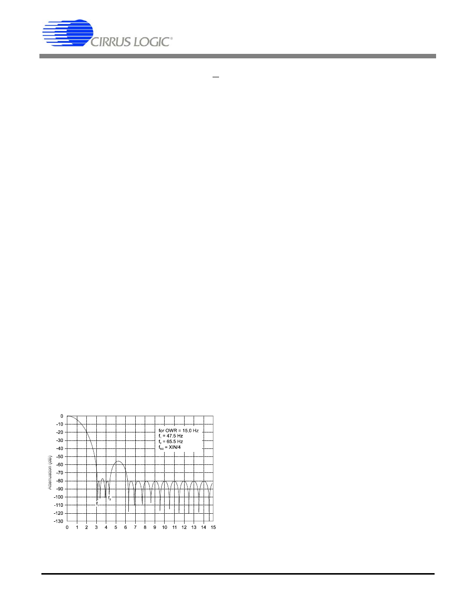
The CS5529 has eight different linear phase digital
filters which set the output word rates (OWRs) as
stated in Configuration Register Descriptions.
These rates assume that XIN is 32.768 kHz. Each
of the filters has a magnitude response similar to
that shown in Figure 5. The filters are optimized to
settle to full accuracy every conversion and yield
better than 80 dB rejection for both 50 Hz and
60 Hz with output word rates at or below 15.0 Sps
(XIN = 32.768 kHz).
The converter’s digital filters scale with XIN. For
example with an output word rate of 15 Sps, the fil-
ter’s corner frequency is typically 12.7 Hz. If XIN
is increased to 64.536 kHz the OWR doubles and
the filter’s corner frequency moves to 25.4 Hz.
Clock Generator
The CS5529 includes a gate which can be connect-
ed with an external crystal to provide the master
clock for the chip. The chip is designed to operate
using a low-cost 32.768 kHz “tuning fork” type
crystal. One lead of the crystal should be connected
to XIN and the other to XOUT. Lead lengths
should be minimized to reduce stray capacitance.
Note that the converter will operate with an exter-
nal (CMOS compatible) clock with frequencies up
to 100 kHz.
Reset System
The reset system bit permits the user to perform a
hardware reset. A hardware reset can be initiated at
any time by writing a logic 1 to the RS (Reset Sys-
tem) bit in the configuration register. After a hard-
ware reset cycle is complete, the serial port logic is
reset and the RV (Reset Valid) bit in the configura-
tion register is set to indicate that a valid reset oc-
curred. After a reset, the on-chip registers are
initialized to the following states and the converter
is placed in the command mode where it waits for
a valid command.
Note:
A system reset can be initiated at any time by
writing a logic 1 to the RS (Reset System) bit
in the configuration register. After a reset, the
RV (Reset Valid) bit is set until the
configuration register is read. The user must
then write a logic 0 to the RS bit to take the
part out of the reset mode.
Figure 5. Filter Response
(Normalized to Output Word Rate = 1).
Configuration Register:
000040(H)
Offset Register:
000000(H)
Gain Register:
400000(H)
