Cirrus Logic CS5529 User Manual
Features, General description

1
Copyright
© Cirrus Logic, Inc. 2005
(All Rights Reserved)
CS5529
16-bit, Programmable
∆Σ ADC with 6-bit Latch
Features
z
Delta-sigma Analog-to-digital Converter
- Linearity Error: 0.0015%FS
- Noise-free Resolution: 16-Bits
z
2.5 V Bipolar/Unipolar Buffered Input Range
z
6-bit Output Latch
z
Eight Digital Filters
- Selectable Output Word Rates
- Output Settles in One Conversion Cycle
- 50/60 Hz ±3 Hz Simultaneous Rejection
z
Simple Three-wire Serial Interface
- SPI™ and Microwire™ Compatible
- Schmitt Trigger on Serial Clock (SCLK)
z
System/Self-calibration with R/W Registers
z
Power Supply Configurations
- VA+ = +5 V; VA- = 0 V; VD+ = +3 V to +5 V
- VA+ = +2.5 V; VA- = -2.5 V; VD+ = +3 V to +5 V
- VA+ = +3.0 V; VA- = -3.0 V; VD+ = +3.0 V
z
Low Power Consumption: 2.6 mW
General Description
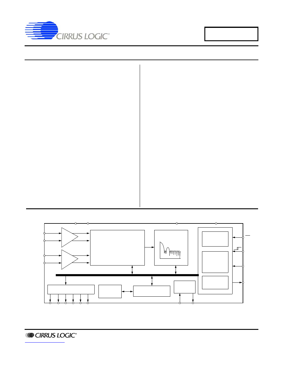
The 16-bit CS5529 is a low-power, programmable
∆Σ
ADC
(Analog-to-Digital Converter), which includes
coarse/fine charge buffers, a fourth-order
∆Σ modulator,
a calibration microcontroller, a digital filter with program-
mable decimation rates, a 6-bit output latch, and a three-
wire serial interface. The ADC is designed to operate
from single or dual analog supplies and a single digital
supply.
The digital filter is programmable with output update
rates between 1.88 Hz to 101 Sps. These output rates
are specified for XIN = 32.768 kHz. Output word rates
can be increased by approximately 3X by using XIN =
100 kHz. The filter is designed to settle to full accuracy
for the selected output word rate in one conversion.
When operated at word rates of 15 Sps or less, the filter
rejects both 50 Hz and 60 Hz simultaneously.
Low power, single conversion settling time, programma-
ble output rates, and the ability to handle negative input
signals make this single- or dual-supply product an ideal
solution for isolated and non-isolated applications.
ORDERING INFORMATION
VA+
AIN+
AIN-
VREF+
VREF-
Latch
A0 A1 D0 D1 D2 D3
Calibration
Memory
Calibration
µC
Clock
Gen.
XIN
XOUT
VA-
DGND
1X
1X
Differential
4th Order
Delta-Sigma
Modulator
Digital Filter
Calibration
Register
Control
Register
Output
Register
VD+
CS
SCLK
SDI
SDO
AUG ‘05
DS246F5
Document Outline
- Features & Descriptions
- General Description
- Table of Contents
- List of Figures
- Characteristics & Specifications
- General Description
- Pin Descriptions
- Specification Definitions
- Ordering Information
- Environmental, Manufacturing, & Handling Information
- Package Dimensions
