Figure 4. adc charge pump regulation loop, An152 – Cirrus Logic AN152 User Manual
Page 3
AN152
AN152REV1
3
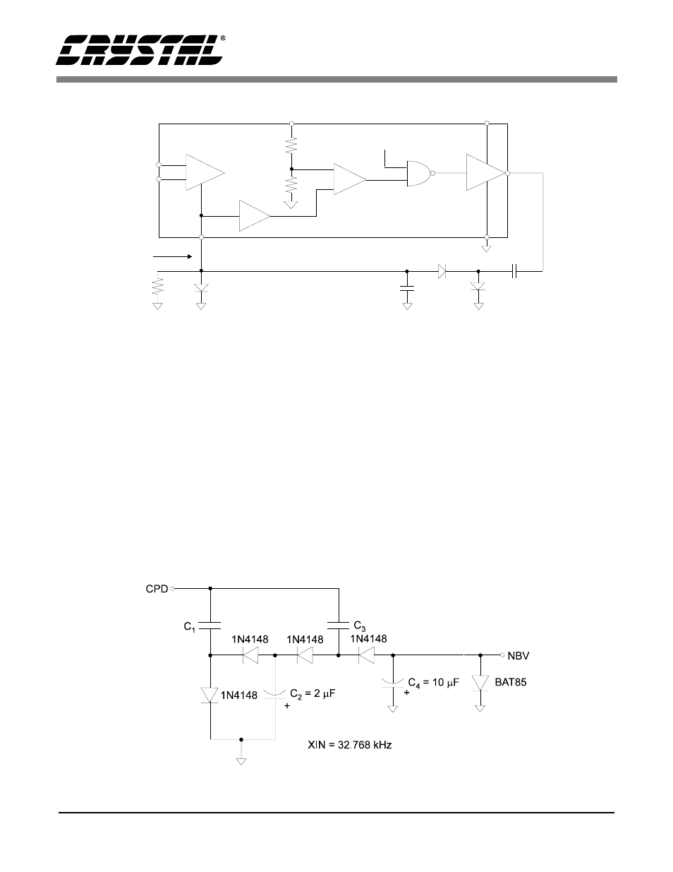
es the proper magnitude, cycles of the charge pump
clock are deleted. The regulation loop maintains
the pulse rate out of the CPD pin at an average fre-
quency that yields the proper output voltage. The
CPD driver output is supplied from the VD+ supply
as shown in Figure 4. This can be +5 V or +3 V.
The diode charge pump shown in Figure 4 is for a
+5 V supply. Diode D3, a Schottky, ensures that the
NBV pin will not go more than a diode drop above
ground. This ensures proper start-up of the regula-
tor loop. Figure 5 illustrates the diode connections
needed if VD+ is 3 V.
Figure 6 illustrates a plot of the average frequency
output from CPD when the external load on the
output of the charge pump is changed. The charge
pump clock (CPCLK) is derived from XIN/2,
therefore the maximum frequency which can be
output from CPD is equal to XIN/2.
The load current in each of the plots exclude the
current used by the on-chip instrumentation ampli-
fier (approximately 450
µ
A for the CS5525/26; 375
µ
A for the CS5521/23; and 700
µ
A for the
CS5522/24/28).
The plot illustrates the average CPD frequency for
two different sizes of charge pump capacitors with
the VA+ supply adjusted to 4.5, 5.0 and 5.5 V. The
NBV
-1x
+
-
CPCLK
+
-
VA+ = 5 V
VD+ = 5 V
CPD
DGND
C
D
R
D
C
D
D , D = 1N4148
D = BAT 85
+
1
2
L
3
1
2
3
2
1
Partial of ADC
Load Current
Extra
Load
Figure 4. ADC Charge Pump Regulation Loop
Figure 5. Charge Pump Drive Diode Circuit For VD+ = 3V