Charge pump basics, Figure 2. charge pump components, Figure 3. charge pump cycle sequence – Cirrus Logic AN152 User Manual
Page 2: The cs552x’s charge pump, An152
AN152
2
AN152REV1
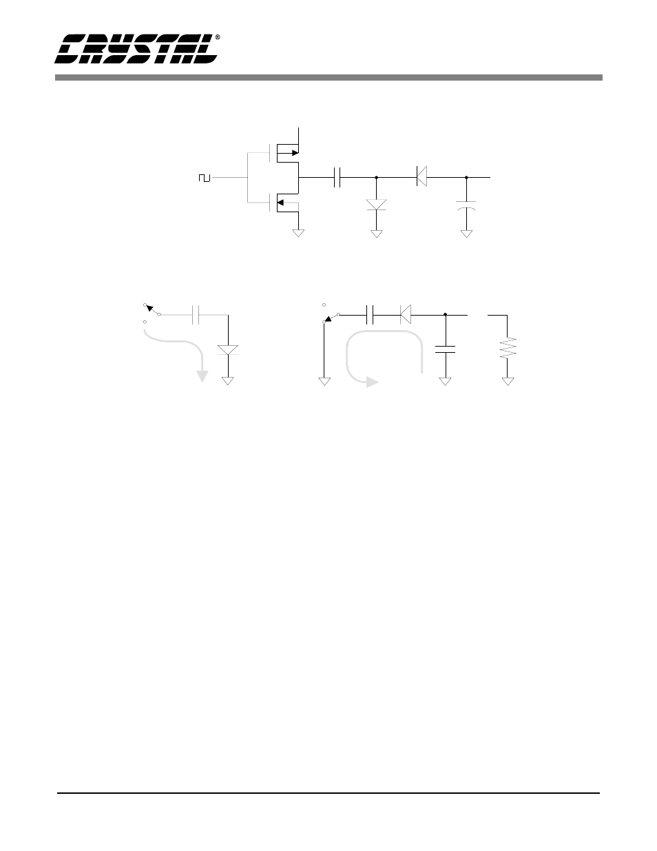
Charge Pump Basics
Figure 2 illustrates a basic diode charge pump.
Transistors Q1 and Q2 represent the output transis-
tors of a CMOS inverter. When the input to the in-
verter causes transistor Q1 to be turned on (Q2 is
off) C1 is charged through diode D1 to a voltage of
approximately 5 V minus the forward voltage of
the diode. When the output of inverter switches to
Q1 off, Q2 on, the positively charged lead of C1
will be connected to ground. Since the voltage
across a capacitor cannot change instantaneously,
the lead of C1 which is connected to diode D2 will
go negative, turning on diode D2. The charge on
C1 will then flow onto C2 and produce a negative
output voltage. Capacitor C2 acts as a reservoir for
charge and is much larger than the charge pump ca-
pacitor C1. After many charge pump cycles, capac-
itor C2 will be charged to a voltage that is about
two diode drops below 5 V.
Figure 3 illustrates each of the two charge pump se-
quences. Capacitor C2 acts as a reservoir for
charge and is much larger than the charge pump ca-
pacitor C1.
The CS552X’s Charge Pump
Figure 4 illustrates a simplified version of the basic
charge pump regulation loop that is inside the A/D
converters listed in this application note. The
charge pump drive pin (CPD) is driven from a
clock (CPCLK) derived from the XIN frequency.
In the CS5525 and CS5526 the XIN frequency is
used directly. The CS5521/22/23/24/28 devices
use a clock that is XIN/2. A regulator loop com-
pares the magnitude of the voltage generated on the
charge reservoir capacitor to a proportion of the
VA+ supply magnitude. The loop is designed to
regulate the voltage at NBV to be -[VA+/2.38] V.
Note that if the VA+ supply voltage to the chip is
above +5 V, the voltage that results out of the
charge pump on NBV will be proportionally more
negative. When the voltage on the NBV pin reach-
D
C
C
1
2
2
Q
Q
D
-V
+
+5 V
Frequency = f
1
2
1
Figure 2. Charge Pump Components
0
V
R
C
D
C
1
2
2
L
I
+
I
D
C
V
(a) (b)
1
1
D
+
-
+ -
Figure 3. Charge Pump Cycle Sequence