Cirrus Logic AN152 User Manual
By bill durbin and jerome johnston introduction, Cs552x overview
1
Copyright
Cirrus Logic, Inc. 1999
(All Rights Reserved)
P.O. Box 17847, Austin, Texas 78760
(512) 445 7222 FAX: (512) 445 7581
http://www.cirrus.com
AN152
Application Note
USING THE CS5521/23, CS5522/24/28, AND CS5525/26
CHARGE PUMP DRIVE FOR EXTERNAL LOADS
By Bill Durbin and Jerome Johnston
INTRODUCTION
The CS5521/23, CS5522/24/28, and CS5525/26
1
series of A/D converters include on-chip circuitry
to drive and regulate a diode charge pump. The
purpose of this application note is to explain the
charge pump circuitry and how it can be used in a
system design.
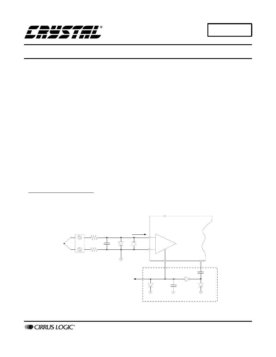
CS552X Overview
The CS5521/23, CS5522/24/28, and CS5525/26
series of A/D converters include a chopper-stabi-
lized instrumentation amplifier for measurement of
low level dc signals (±100 mV or less). This ampli-
fier is designed to produce very low input sampling
current (I
CVF
< 300 pA over -40 to +85 C). A low
input current minimizes the errors that can occur in
thermocouple measurements when high impedance
circuitry is used for input protection as shown in
Figure 1.
The charge pump circuitry, illustrated in Figure 1,
is used to generate a negative supply (approximate-
ly -2.1 V) to power the on-chip instrumentation
amplifier. This enables the amplifier to measure
low level input signals that are negative relative to
ground while maintaining low input current. With-
in certain constraints, which are described in this
document, the charge pump can be used to power
some additional circuitry outside the converter,
such as an amplifier or a multiplexer.
1.The CS5529 is not included in this Application
Note because it does not contain a charge pump.
0.1 uF
+
-
VA+
CS5521/23,
CS5522/24/28,
& CS5525/26
NBV
CPD
1N4148
+
BAT85
External Load
T/C
10 K
Ve
+
-
10 K
I
1N4148
Charge Pump Circuit
Figure 1. Input Amplifier inside CS552x ADCs.
AUG ‘99
AN152REV1
Document Outline
- AN152: USING THE CS552X’S CHARGE PUMP DRIVE FOR EXTERNAL LOADS
- INTRODUCTION
- CS552X Overview
- Charge Pump Basics
- The CS552X’s Charge Pump
- Figure 4. ADC Charge Pump Regulation Loop
- Figure 5. Charge Pump Drive Diode Circuit For VD+ = 3V
- Figure 6. Load Current vs. Frequency for the CS5521/23 and CS5522/24/28; VA+ = VD+
- Figure 7. Load Current vs. Frequency for the CS5525/26; VA+ = VD+
- Figure 8. Load Current vs. Frequency; VA+ = VD+ = 5 V, Capacitor Size = 0.15 uF; CS5521/22/23/24/28
- Figure 9. Load Current vs. Frequency for VD+ = 3.0 V, Capacitor Sizes = 0.47 uF CS5521/22/23/24/28
- Figure 10. Load Current vs. Frequency for VA+ = 5.0 V, Capacitor Sizes = 0.47 uF CS5521/22/23/24/28
- Running the CS552X at Frequencies other than 32.768 kHz
- APPENDIX
- INTRODUCTION