3 transfer data to/from adc, Figure 3. bit representation/storage in 80c51, 4 transfer data to/from pc – Cirrus Logic AN118 User Manual
Page 3: An118
AN118
AN118REV2
3
final byte with its LSB at logic 0 are needed to reset
the serial port). This places the ADC in the com-
mand state, where it awaits a valid command. Fi-
nally, before returning to the main routine, the
mode pin is queried to determine whether a three or
four-wire interface is being used.
3.3 Transfer Data To/From ADC
Transferring data to and from the ADC is done
through the transfer_byte and receive_byte func-
tions. Transfer_byte takes one byte of input and
sends it to the ADC one bit at a time (MSB first) by
applying the bit information to P1.1 (SDI) and then
pulsing P1.3 (SCLK). This is repeated eight times
to transfer the entire byte of data to the ADC.
Receive_byte works in just the opposite direction,
obtaining byte information MSB-first on the P1.2
(SDO) line as it provides the clock on P1.3. The
functions write_to_register and read_register
make use of these byte transfer functions to send
and receive internal register information in the
proper order from the ADC. Write_to_register
writes four bytes of information to the ADC using
transfer_byte. The command byte is written first,
followed by the high, middle, and low bytes of the
24-bit register word. Read_register, on the other
hand, sends a command byte to the ADC using
transfer_byte, and then obtains the 24-bit register
word by calling receive_byte three times in succes-
sion. Due to the conversion time delay, reading
conversion data requires a slightly different method
than reading register information. The
read_conversion algorithm is designed for this pur-
pose. The configuration register is read and stored
in memory using the read_register command. The
LP, RC, and MC bits are then masked to zero, and
the register is written using write_to_register. The
command to start a conversion is then written using
transfer_byte, and SDO is polled until the ADC in-
dicates that the conversion is complete. Once a val-
id conversion has been obtained, eight zeros are
sent to the ADC with transfer_byte to start the
transfer of data, at which time receive_byte is
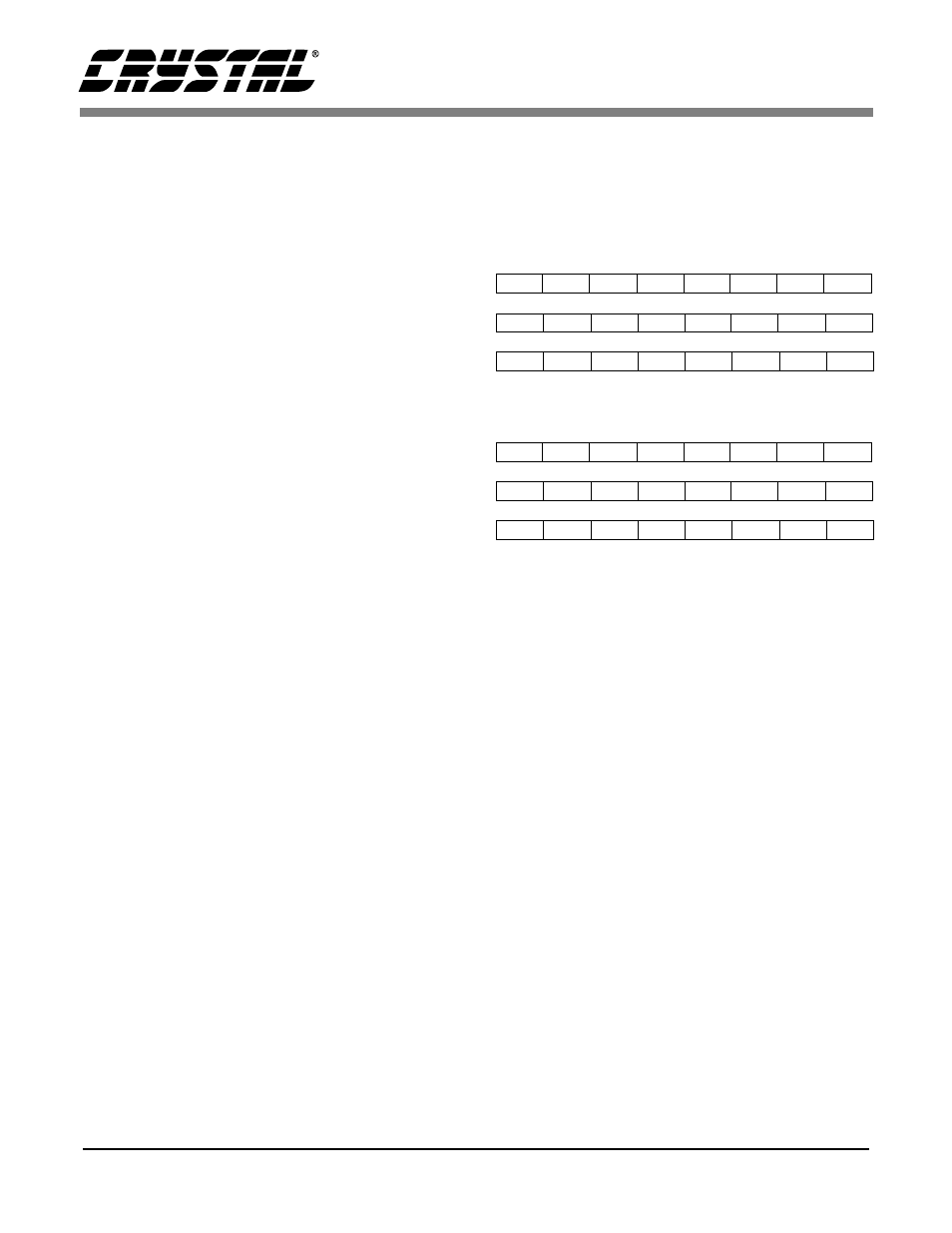
called three times to obtain the data word (see Fig-
ure 3 for more detail on how the information is or-
ganized among the three bytes) Figure 6 shows the
conversion data timing.
3.4 Transfer Data To/From PC
Transferring data to and from a PC through the
80C51’s serial port is accomplished with the rou-
tines txser and rxser. These two routines rely upon
status bits in the 80C51’s Serial Control Register
(SCON, located at address 0x98 Hex). Txser trans-
fers data to the serial port by first polling TI (Trans-
fer Interrupt, bit 1 in SCON) until the 80C51’s
serial buffer is empty, and ready to receive infor-
mation. Once TI is at a logic high level, the soft-
ware clears the TI bit and moves the byte to be
transferred into the 80C51’s serial buffer, where it
is transmitted to the PC LSB first. Rxser receives a
byte in a similar fashion, by polling RI (Receive In-
terrupt, bit 0 in SCON) until there is valid data
available in the 80C51’s serial buffer. When RI is
at a logic high level, the data is transferred out of
the serial buffer to an immediate memory location.
MSB
High-Byte
Mid-Byte
Low-Byte
A) 24-bit Conversion Data Word (CS5522/24/28)
MSB
High-Byte
Mid-Byte
Low-Byte
B) 16-bit Conversion Data Word (CS5521/23)
0 - always zero, 1 - always 1
CI1, CI0 - Channel Indicator Bits
OD - Oscillation Detect, OF - Overflow
Figure 3. Bit Representation/Storage in 80C51
D23
D22
D21
D20
D19
D18
D17
D16
D15
D14
D13
D12
D11
D10
D9
D8
D7
D6
D5
D4
D3
D2
D1
D0
D15
D14
D13
D12
D11
D10
D9
D8
D7
D6
D5
D4
D3
D2
D1
D0
1
1
1
0
CI1
CI0
OD
OF