4 digital section, 5 power supply section, 4 digital section 1.5 power supply section – Cirrus Logic CDB5463U User Manual
Page 5: Cdb5463u, Table 4
CDB5463U
DS805DB2
5
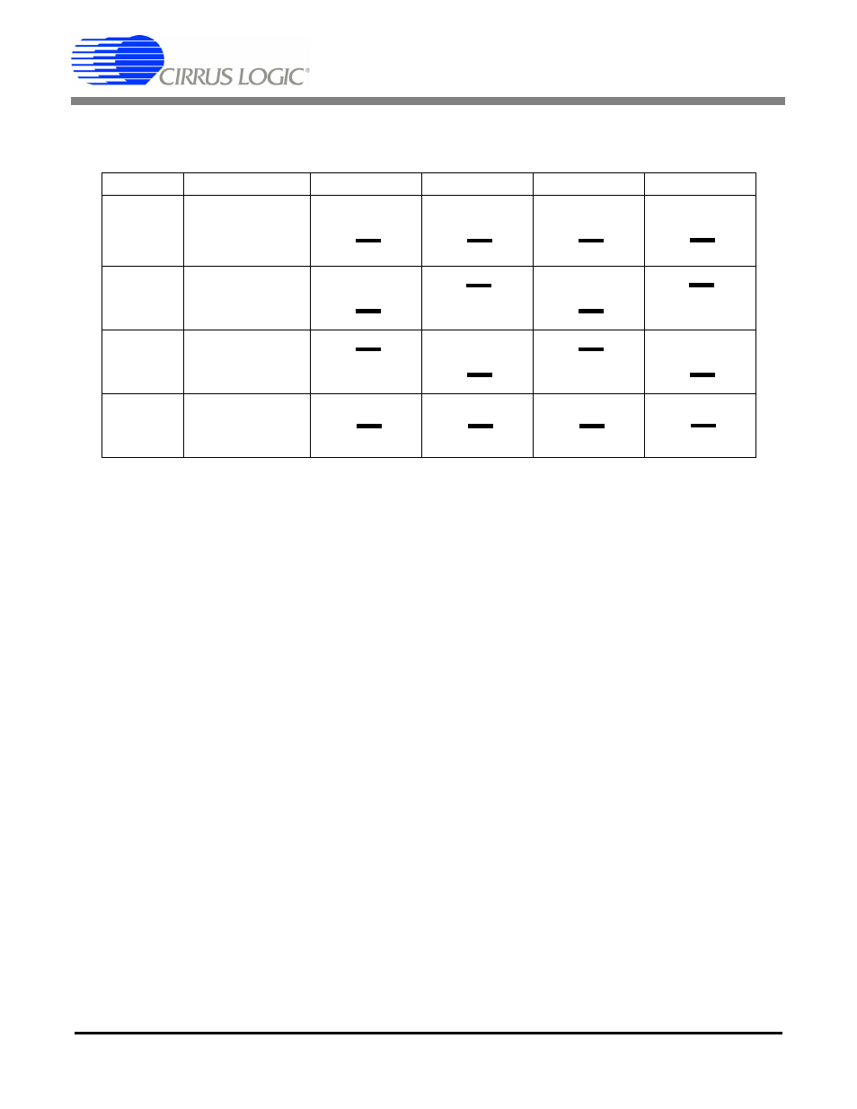
J26 in the GND position, the inputs are connected to analog ground (AGND). With a jumper on J17, J22,
J24 and J26 in position VREF, the inputs are connected to the reference voltage selected on J12.
1.4
Digital Section
The digital section contains the microcontroller, USB interface, JTAG header, reset circuitry, and an ex-
ternal interface header (J40). The microcontroller interfaces the SPI of CS5463 with the USB connection
to the PC, enabling the GUI software to access all the CS5463 registers and functions. Interface header,
J40, is provided to allow the CDB5463U to be connected to an external energy registration device or an
external microcontroller. To connect the CS5463 to an external microcontroller, R57, R58, R59, R60, R61,
and R62 must be removed from the board. The energy output pins E1, E2, and E3 are routed to LEDs
which provide a simple visual check of the energy output pulses. The MODE pin is also routed to a LED
to indicate whether the CS5463 is operating in auto-boot mode. Jumpers J10, J13, J15, and J16 are
equipped at the factory with jumpers to enable the LEDs.
1.5
Power Supply Section
Table 4
illustrates the power supply connections to the evaluation board. The +5V binding post (J3) sup-
plies the positive analog (VA+) for the CS5463 and the +2.5V reference. The VD+_EXT binding post (J5)
supplies the digital section of the CS5463 (VD+) and level shifters. Jumper J8 allows the VD+ supply to
be sourced from the VD+_EXT binding post (J5), the +5V binding post (J3), or the regulated 3.3V supply
derived from the microcontroller. The Vu+_EXT (J6) binding post supplies the positive supply for the 8051
INPUT
Description
J17
J22
J24
J26
VIN± or IIN±
Selects External
Signal
VIN± or IIN±
Selects External
Signal
GND
Selects Grounding
the Input
VREFIN
Selects Reference
Source
Table 3. Voltage and Current Channel Input Signal Selection
O
VIN+
O O
VIN+
O O
VIN+
GND
VREF
VIN+
(Default)
O
VIN-
O O
VIN-
O O
VIN-
VIN-
VREF
GND
(Default)
O
IIN+
O O
IIN+
O O
IIN+
GND
VREF
IIN+
(Default)
O
IIN-
O O
IIN-
O O
IIN-
IIN-
VREF
GND
(Default)
O
VIN+
O O
VIN+
O O
VIN+
GND
VREF
VIN+
O
VIN-
O O
VIN-
O O
VIN-
VIN-
VREF
GND
O
IIN+
O O
IIN+
O O
IIN+
GND
VREF
IIN+
O
IIN-
O O
IIN-
O O
IIN-
IIN-
VREF
GND
O
VIN+
O O
VIN+
O O
VIN+
GND
VREF
VIN+
O
VIN-
O O
VIN-
O O
VIN-
VIN-
VREF
GND
O
IIN+
O O
IIN+
O O
IIN+
GND
VREF
IIN+
O
IIN-
O O
IIN-
O O
IIN-
IIN-
VREF
GND
O
VIN+
O O
VIN+
O O
VIN+
GND
VREF
VIN+
O
VIN-
O O
VIN-
O O
VIN-
VIN-
VREF
GND
O
IIN+
O O
IIN+
O O
IIN+
GND
VREF
IIN+
O
IIN-
O O
IIN-
O O
IIN-
IIN-
VREF
GND