5 pcb layout, 1 layer stack, 2 differential pairs – Cirrus Logic CDB5374 User Manual
Page 32: 1 layer stack 2.5.2 differential pairs, Figure 4. differential pair routing, Cdb5374
CDB5374
32
DS862DB1
The VD and VCORE power supplies on CDB5374 include reverse-biased Schottky diodes to ground to
protect against reverse voltages that could latch-up the CMOS components. Also included on VD and
VCORE are 100 uF bulk capacitors for bypassing and to help settle transients plus individual 0.1 uF by-
pass capacitors local to the digital power supply pins of each device.
2.5
PCB Layout
2.5.1
Layer Stack
CDB5374 layers 1 and 2 are dedicated as analog routing layers. All critical analog signal routes are on
these two layers. Some CPLD and microcontroller digital routes are also included on these layers away
from the analog signal routes.
CDB5374 layer 3 is dedicated for power supply routing. Each power supply net includes at least 100 µF
bulk capacitance as a charge well for settling transient current loads.
CDB5374 layer 4 is a solid ground plane without splits or routing. A solid ground plane provides the best
return path for bypassed noise to leave the system. No separate analog ground is required since analog
signals on CDB5374 are differentially routed.
CDB5374 layers 5 and 6 are dedicated as digital routing layers.
2.5.2
Differential Pairs
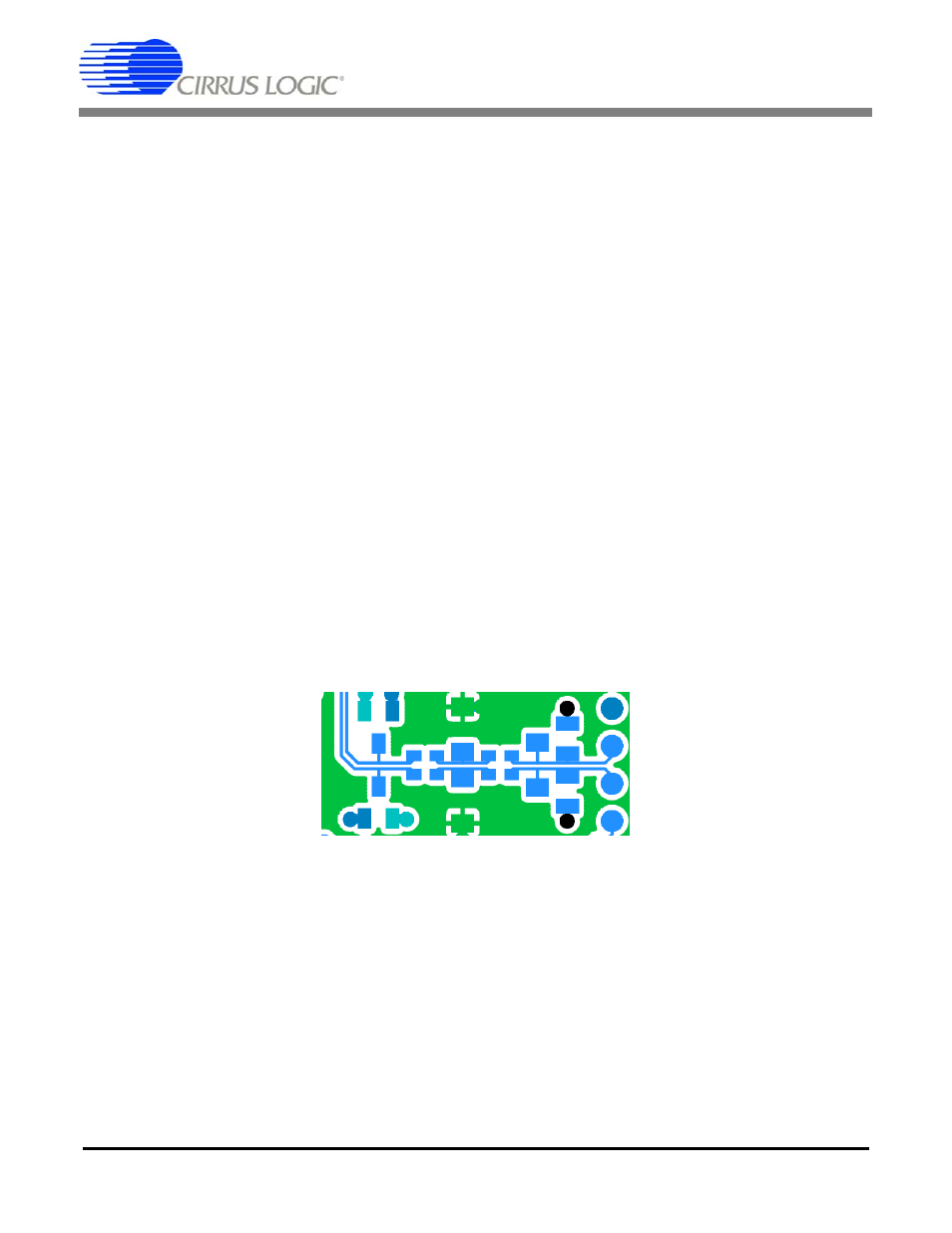
Analog signal routes on CDB5374 are differential with dedicated + and - traces. All source and return an-
alog signal currents are constrained to the differential pair route and do not return through the ground
plane. Differential traces are routed together with a minimal gap between them so that noise events affect
them equally and are rejected as common mode noise.
Analog signal connections into the CS5374 amplifiers are 2-wire IN+ and IN- differential pairs, and are
routed as such. Analog signal connections out of the amplifiers and into the modulators are externally sep-
Figure 4. Differential Pair Routing
IN+
IN-