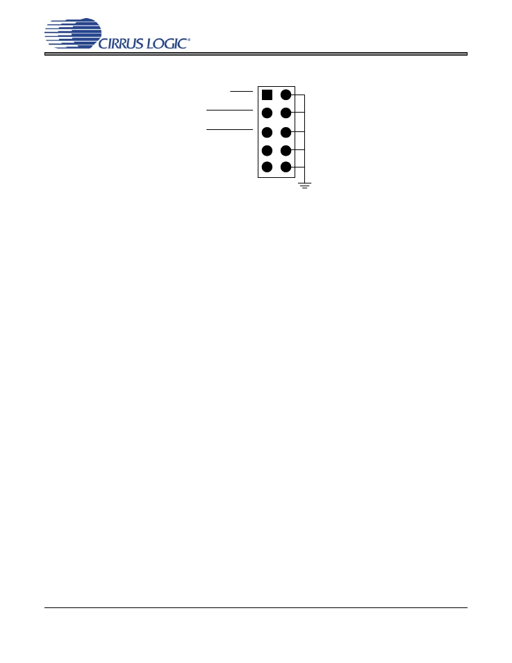
Figure 7. status indicator and reset header, j16, 6 analog inputs, 7 power – Cirrus Logic CRD5381 User Manual
Page 11: 8 grounding and power supply decoupling, Crd5381
DS563RD1
11
CRD5381
Figure 7. Status Indicator and Reset Header, J16
2.6
Analog Inputs
The CRD5381 provides four fully differential analog inputs via J9, J11, J7, and J12; shown in
and
. Each analog input has the required analog circuitry to optimize the performance of each CS5381.
The input buffer to each CS5381 device has unity gain, and the CRD5381 differential input amplitude re-
quired to generate a full-scale digital output is typically 5.65 Vpp.
If extra analog input circuitry is required in the user’s design, it should drive a buffer equivalent to the con-
tents of the dotted boxes shown in
and in
labeled “CS5381 Required Input Circuitry”. In
this case, all components outside the dotted boxes in
and
design.
2.7
Power
The CRD5381 requires the user to supply +3.3 V (J6) and ±12 V (J2 and J1) to the board. Onboard regula-
tors supply the required +5 V and +2.5 V. All voltage inputs must be referenced to the single black banana-
type ground connector (J5). Zener Diodes Z1 and Z2 (shown in
) are used to protect the CRD5381
circuitry from accidental connection of a reversed polarity supply or a supply of over ± 13 V to J1 and J2.
WARNING: Please refer to the CS5381 and CS8421 data sheet for allowable voltage levels.
2.8
Grounding and Power Supply Decoupling
The CS5381 and CS8421 require careful attention to power supply and grounding arrangements in order
to optimize performance.
provides an overview of the connections on the CRD5381;
shows the component placement.
shows the top layout,
shows the bottom layout,
shows the ground plane. The decoupling capacitors are lo-
cated as close to the CS5381 and CS8421 as possible. Extensive use of ground plane fill in the evaluation
board yields large reductions in radiated noise.
OVERFLOW A
OVERFLOW B
SRC UNLOCK A
RESET
Signal
Ground
J16
SRC UNLOCK B