Pin description – Cirrus Logic CS5340 User Manual
Page 13
DS601F2
13
CS5340
Confidential Draft
3/11/08
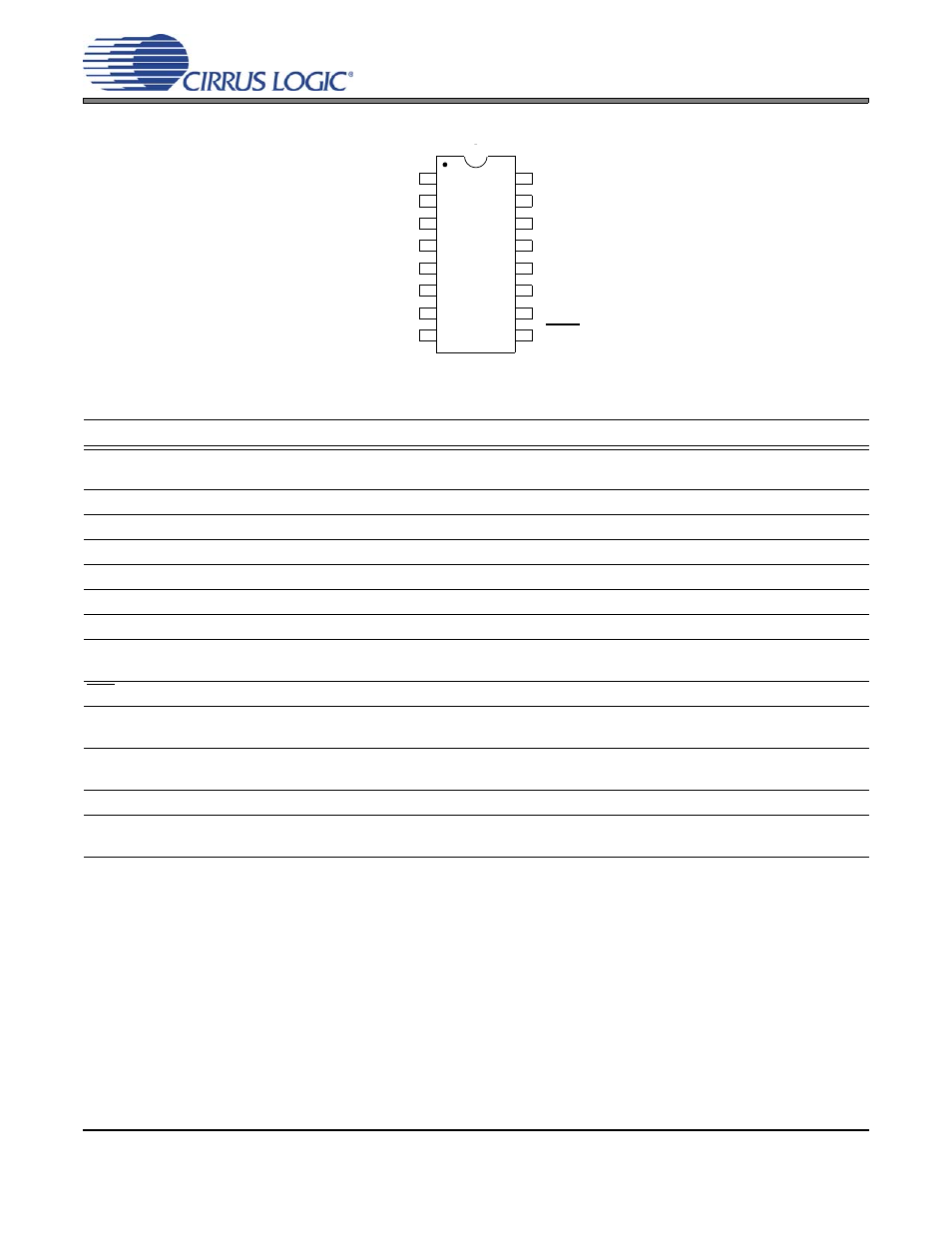
2. PIN DESCRIPTION
Pin Name
#
Pin Description
M0
M1
1
16
Mode Selection (Input) - Determines the operational mode of the device.
MCLK
2
Master Clock (Input) - Clock source for the delta-sigma modulator and digital filters.
VL
3
Logic Power (Input) - Positive power for the digital input/output.
SDOUT
4
Serial Audio Data Output (Output) - Output for two’s complement serial audio data.
GND
5,14
Ground (Input) - Ground reference. Must be connected to analog ground.
VD
6
Digital Power (Input) - Positive power supply for the digital section.
SCLK
7
Serial Clock (Input/Output) - Serial clock for the serial audio interface.
LRCK
8
Left Right Clock (Input/Output) - Determines which channel, Left or Right, is currently
active on the serial audio data line.
RST
9
Reset (Input) - The device enters a low power mode when low.
AINL
AINR
10
12
Analog Input (Input) - The full-scale analog input level is specified in the Analog Charac-
teristics specification table.
VQ
11
Quiescent Voltage (Output) - Filter connection for the internal quiescent
reference voltage.
VA
13
Analog Power (Input) - Positive power supply for the analog section.
FILT+
15
Positive Voltage Reference (Output) - Positive reference voltage for the internal
sampling circuits.
M0
M1
MCLK
FILT+
VL
REF_GND
SDOUT
VA
GND
AINR
VD
VQ
SCLK
AINL
LRCK
RST
1
2
3
4
5
6
7
8
5
1
2
6
16
15
14
13
12
11
10
9
1
2
3
4
5
6
7
8
5
1
2
6
16
15
14
13
12
11
10
9