Cirrus Logic CDB5331A User Manual
Cirrus Logic Hardware

Features
•
Demonstrates recommended layout
and grounding arrangements
•
CS8402A Generates AES/EBU, S/PDIF,
& EIAJ-340 Compatible Digital Audio
•
Buffered Serial Output Interface
•
Digital and Analog Patch Areas
•
On-board or externally supplied system
timing
General Description
The CDB5330A/31A evaluation board is an excellent
means for quickly evaluating the CS5330A/31A 18-bit,
stereo A/D converter. Evaluation requires a digital
signal processor, a low distortion analog signal
source and a power supply. Analog inputs are pro-
vided via RCA connectors for both channels.
Also included is a CS8402A digital audio interface
transmitter which generates AES/EBU, S/PDIF, and
EIAJ-340 compatible audio data. The digital audio data
is available via RCA phono, and optical connectors.
The evaluation board may also be configured to accept
external timing signals for operation in a user applica-
tion during system development.
ORDERING INFORMATION: CDB5330A, CDB5331A
Evaluation Board for CS5330A / CS5331A
CDB5330A
CDB5331A
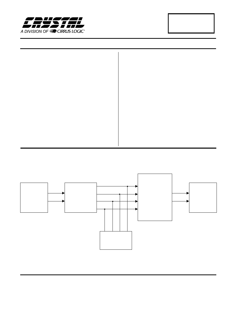
Analog
Filter
Digital
Audio
Output
CS8402A
Digital
Audio
Interface
CS5330A/31A
I/O for Clocks
and Data
Cirrus Logic, Inc.
Crystal Semiconductor Product Division
P.O. Box 17847, Austin, TX 78760
(512) 445-7222 FAX: (512) 445-7581
http://www.crystal.com
OCT ’97
DS138DB2
17
Copyright
Cirrus Logic, Inc. 1997
(All Rights Reserved)
Document Outline
- CDB5330A CDB5331A Evaluation Board for CS5330A / CS5331A
- Features
- General Description
- ORDERING INFORMATION:
- CDB5330A/31A System Overview
- CS5330A/31A Analog to Digital Converter
- CS8402A Digital Audio Interface
- CS8402A Data Format
- Analog input buffer
- Power Supply Circuitry
- Input/Output for Clocks and Data
- Grounding and Power Supply Decoupling
- Table 1. System Connections
- Table 2. CDB5330A Jumper Selectable Options
- Table 3. CDB5331A Jumper Selectable Options
- Table 4. CS8402A Switch Definitions - Consumer Mode
- Table 5. CS8402A Switch Definitions - Professional Mode
- Figure 1. System Block Diagram and Signal Flow
- Figure 2. CS5330A/ 31A and Connections
- Figure 3. MCLK Generation and Power Down
- Figure 4. CS8402A Digital Audio Transmitter Connections
- Figure 5. I/O Interface for Clocks and Data
- Figure 6. Power Supply
- Figure 7. CDB5330A/31A Component Side Silkscreen
- Figure 8. CDB5330A/31A Component Side (top)
- Figure 9. CDB5330A/31A Solder Side (bottom)
