3 cdb48500 system description, Chapter 3. cdb48500 system description -1, Figure 3-1. cdb48500 block diagram -1 – Cirrus Logic CDB48500-USB User Manual
Page 15
1
Chapter 3
CDB48500 System Description
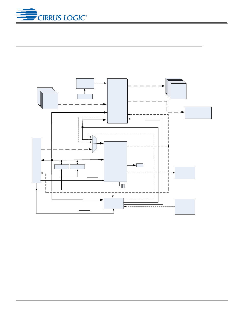
A detailed block diagram of the CDB48500 Customer Development Board is shown in
. The sections
that follow provide a detailed description of each block.
Figure 3-1. CDB48500 Block Diagram
CS42448_RESET
Co
ntr
o
l He
ad
er
– J
1
1
CS42448
CS485XX
CS8416
MIC In
MIC
Preamp
S/PDIF
In
S/PDIF
Out
USB Clocks/Data
SPI FLASH
LED
WDO
DSP_RESET
BRD_RESET
1
0
ADC Data
S/PDIF Data
Audio Clocks
SPDIF IN
SPDIF OUT
SPI / I2C
XT
A
L
_O
U
T
Analog
In
Analog
In
Analog
In
Analog
In
Analog
In
Up to 12
Analog
Inputs
Analog
In
Analog
In
Analog
In
Analog
In
Analog
In
Up to 12
Analog
Outputs
2x
CS42448
I2C FLASH
Headphone
Out
DAO Audio Out
DAO Audio Out
DAO[3]
See also other documents in the category Cirrus Logic Hardware:
- CobraNet (147 pages)
- CS4961xx (54 pages)
- CS150x (8 pages)
- CS1601 (2 pages)
- CS1501 (16 pages)
- CS1601 (16 pages)
- CS1610 (16 pages)
- CRD1610-8W (24 pages)
- CRD1611-8W (25 pages)
- CDB1610-8W (21 pages)
- CS1610A (18 pages)
- CDB1611-8W (21 pages)
- CDB1610A-8W (21 pages)
- CDB1611A-8W (21 pages)
- CRD1610A-8W (24 pages)
- CRD1611A-8W (25 pages)
- CS1615 (16 pages)
- AN403 (15 pages)
- AN401 (14 pages)
- AN400 (15 pages)
- AN375 (27 pages)
- AN376 (9 pages)
- CRD1615-8W (22 pages)
- CRD1616-8W (23 pages)
- AN402 (14 pages)
- AN404 (15 pages)
- CRD1615A-8W (21 pages)
- CS1615A (16 pages)
- CS1630 (56 pages)
- AN374 (35 pages)
- AN368 (80 pages)
- CRD1630-10W (24 pages)
- CRD1631-10W (25 pages)
- CS1680 (16 pages)
- AN405 (13 pages)
- AN379 (31 pages)
- CRD1680-7W (31 pages)
- AN335 (10 pages)
- AN334 (6 pages)
- AN312 (14 pages)
- AN Integrating CobraNet into Audio Products (16 pages)
- CobraNet Audio Routing Primer (9 pages)
- Bundle Assignments in CobraNet Systems (3 pages)
- CS2300-01 (3 pages)
- CS2000-CP (38 pages)