Voltage reference, 1 vref power supply, 2 vref rc filter – Cirrus Logic CS4373A User Manual
Page 26: 3 vref pcb routing, Figure 13. voltage reference circuit, Cs4373a, Routing, Bypass
CS4373A
26
DS699F2
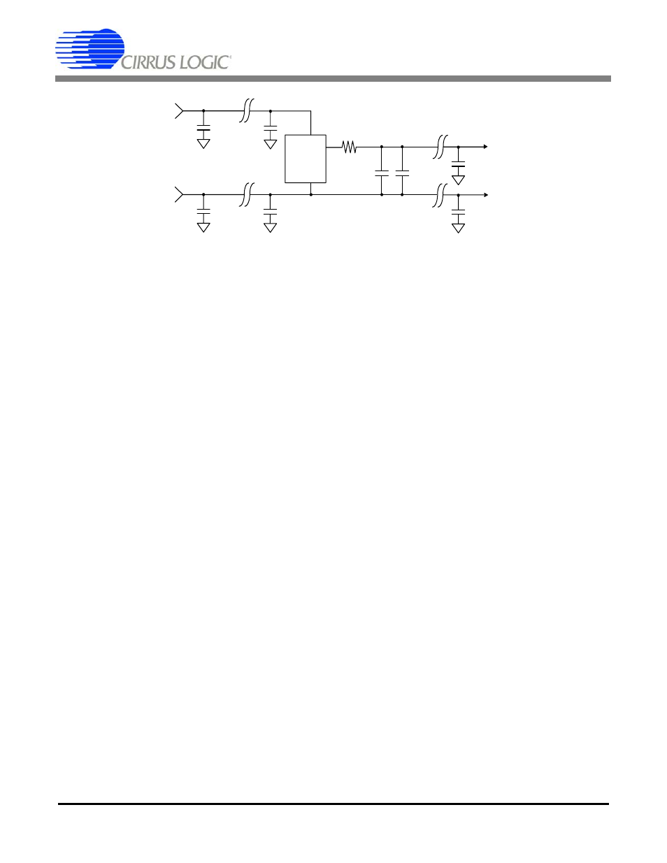
8. VOLTAGE REFERENCE
The CS4373A requires a 2.500 V precision
voltage reference to be supplied to the VREF
±
pins.
8.1 VREF Power Supply
To guarantee proper regulation headroom for
the voltage reference device, the voltage refer-
ence GND pin should be connected to VA- in-
stead of system ground, as shown in
. This connection results in VREF-
voltage equal to VA- and VREF+ voltage very
near ground potential [(VA-) + 2.500 VREF].
Power supply inputs to the voltage reference
device should be bypassed to system ground
with 0.1
µF capacitors placed as close as pos-
sible to the power and ground pins. In addition
to 0.1
µF local bypass capacitors, at least
100
µF of bulk capacitance to system ground
should be placed on each power supply near
the voltage regulator outputs. Bypass capaci-
tors should be X7R, C0G, tantalum, or other
high-quality dielectric type.
8.2 VREF RC Filter
Linear Technol-
ogy LT1019AIS8-2.5
voltage reference yields
acceptable noise levels if the output is filtered
with a low-pass RC filter.
A separate RC filter is required for each sys-
tem device connected to a given voltage refer-
ence. By sharing a common RC filter, signal-
dependent sampling of the voltage reference
by one system device could cause unwanted
tones to appear in the measurement band-
width of another system device via common
impedance coupling.
8.3 VREF PCB Routing
To minimize the possibility of outside noise
coupling into the CS4373A voltage reference
input, the VREF
±
traces should be routed as a
differential pair from the large capacitor of the
voltage reference RC filter. Careful control of
the voltage reference source and return cur-
rents by routing VREF
±
as a differential pair
will improve immunity from external noise.
To further improve noise rejection of the
VREF
± routing,
include 0.1
µF
bypass
ca-
pacitors to system ground as close as possible
to the VREF+ and VREF- pins of the
CS4373A.
10
Ω
To VREF+
+
To VA+
Regulator
2.500 V
VREF
0.1
µF
To VREF-
0.1
µF
100
µF
0.1
µF
0.1
µF
0.1
µF
100
µF
100
µF
To VA-
Regulator
Route VREF
±
as a differential pair
from the 100uF RC filter capacitor
Figure 13. Voltage Reference Circuit