Digital inputs, 1 tdata connection, 2 mclk connection – Cirrus Logic CS4373A User Manual
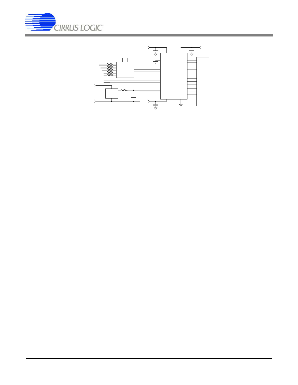
Page 22: 3 msync connection, Figure 11. digital inputs, Cs4373a, For mea
CS4373A
22
DS699F2
6. DIGITAL INPUTS
The CS4373A is designed to operate with the
CS5376A digital filter. The digital filter gener-
ates one-bit
∆Σ test bit stream data (TDATA),
a master clock (MCLK) and a synchronization
signal (MSYNC). In addition, the digital filter
GPIO pins control the CS4373A operational
mode (MODE) and attenuator (ATT) settings.
6.1 TDATA Connection
The TDATA digital input expects encoded
one-bit
∆Σ data nominally at a 256 kHz rate.
The one’s density input range is approximately
25% minimum to 75% maximum, with differen-
tial mid-scale at 50% one’s density.
The CS5376A digital filter test bit stream
(TBS) generator can encode two types of AC
signals as over-sampled, one-bit
∆Σ data - a
pure sine wave for THD and CMRR testing or
a triggerable impulse waveform for synchroni-
zation testing and impulse response charac-
terization. In the AC operational modes, the
CS4373A converts the over-sampled bit
stream digital data into precision differential or
common mode analog AC signals.
The CS5376A TBS sine mode encodes an ap-
proximately 5 V
pp
full-scale sine wave signal
with a digital filter TBSGAIN register setting of
0x04B8F2. Because TBS impulse mode en-
codes frequencies above 100 Hz, a maximum
0x0078E5 TBSGAIN impulse mode register
setting is specified to guarantee stability of the
CS4373A low-power
∆Σ circuitry. Details on
the setup and operation of the digital filter TBS
generator can be found in the CS5376A data
sheet.
6.2 MCLK Connection
The CS5376A digital filter generates the mas-
ter clock for CS4373A, typically 2.048 MHz,
from a synchronous CLK input from the exter-
nal system. By default, MCLK is disabled at re-
set and is enabled by writing the digital filter
CONFIG register. If MCLK is disabled during
operation, the CS4373A will enter power down
after approximately 40
µ
S.
MCLK must have low in-band jitter to guaran-
tee full analog performance, requiring a crys-
tal- or VCXO-based system clock into the
digital filter. Clock jitter on the digital filter ex-
ternal CLK input directly translates to jitter on
MCLK.
6.3 MSYNC Connection
The CS5376A digital filter also provides a syn-
chronization signal to the CS4373A. The
MSYNC signal is generated following a rising
edge received on the digital filter SYNC input.
By default MSYNC generation is disabled at
reset and is enabled by writing to the digital fil-
ter CONFIG register.
The input SYNC signal to the CS5376A digital
filter sets a common reference time t
0
for mea-
CS4373A
TDATA
CAP+
CAP-
BUF+
BUF-
OUT+
OUT-
MCLK
MSYNC
DGND
MODE1
MODE2
ATT0
ATT1
MODE0
ATT2
VA-
2.5 V
VREF
10
Ω
VREF+
VREF-
100µF
VA+
VA-
VD
0.1µF
0.1µF
VD
VA+
10nF
C0G
Analog
Switches
CH1 BUF
CH2 BUF
CH3 BUF
CH4 BUF
CH1,2,3,4 OUT
SWITCH
CONTROL
GPIO
CS5376A
SIGNALS
MCLK
MSYNC
TBSDATA
GPIO
GPIO
GPIO
GPIO
GPIO
ELECTRONICS
SENSOR
VA-
0.1µF
VA-
+
Route VREF as diff pair
Route OUT as diff pair
Route BUF as diff pair
Figure 11. Digital Inputs