Figure 9. control port timing, i·c mode, 3 spi mode, Figure 9. control port timing, i²c mode – Cirrus Logic CS4351 User Manual
Page 21: Figure 9, Cs4351, 2 i²c read, 1 spi write
DS566F1
21
CS4351
4.9.2.2
I²C Read
To read from the device, follow the procedure below while adhering to the control port Switching Specifica-
tions.
1. Initiate a START condition to the I²C bus followed by the address byte. The upper 6 bits must be
100110. The seventh bit must match the setting of the AD0 pin, and the eighth must be 1. The eighth
bit of the address byte is the R/W bit.
2. After transmitting an acknowledge (ACK), the device will then transmit the contents of the register
pointed to by the MAP. The MAP register will contain the address of the last register written to the
MAP, or the default address (see
) if an I²C read is the first operation performed on
the device.
3. Once the device has transmitted the contents of the register pointed to by the MAP, issue an ACK.
4. If the INCR bit is set to 1, the device will continue to transmit the contents of successive registers.
Continue providing a clock and issue an ACK after each byte until all the desired registers are read,
then initiate a STOP condition to the bus.
5. If the INCR bit is set to 0 and further I²C reads from other registers are desired, it is necessary to
initiate a repeated START condition and follow the procedure detailed from steps 1 and 2 from the
I²C Write instructions followed by step 1 of the I²C Read section. If no further reads from other reg-
isters are desired, initiate a STOP condition to the bus.
4.9.3
SPI Mode
In SPI mode, data is clocked into the serial control data line, CDIN, by the serial control port clock, CCLK
(see
for the clock to data relationship). There is no AD0 pin. Pin CS is the chip select signal and
is used to control SPI writes to the control port. When the device detects a high to low transition on the
AD0/CS pin after power-up, SPI mode will be selected. All signals are inputs and data is clocked in on the
rising edge of CCLK.
4.9.3.1
SPI Write
To write to the device, follow the procedure below while adhering to the control port Switching Specifica-
tions in
.
1. Bring CS low.
2. The address byte on the CDIN pin must then be 10011000.
3. Write to the memory address pointer, MAP. This byte points to the register to be written.
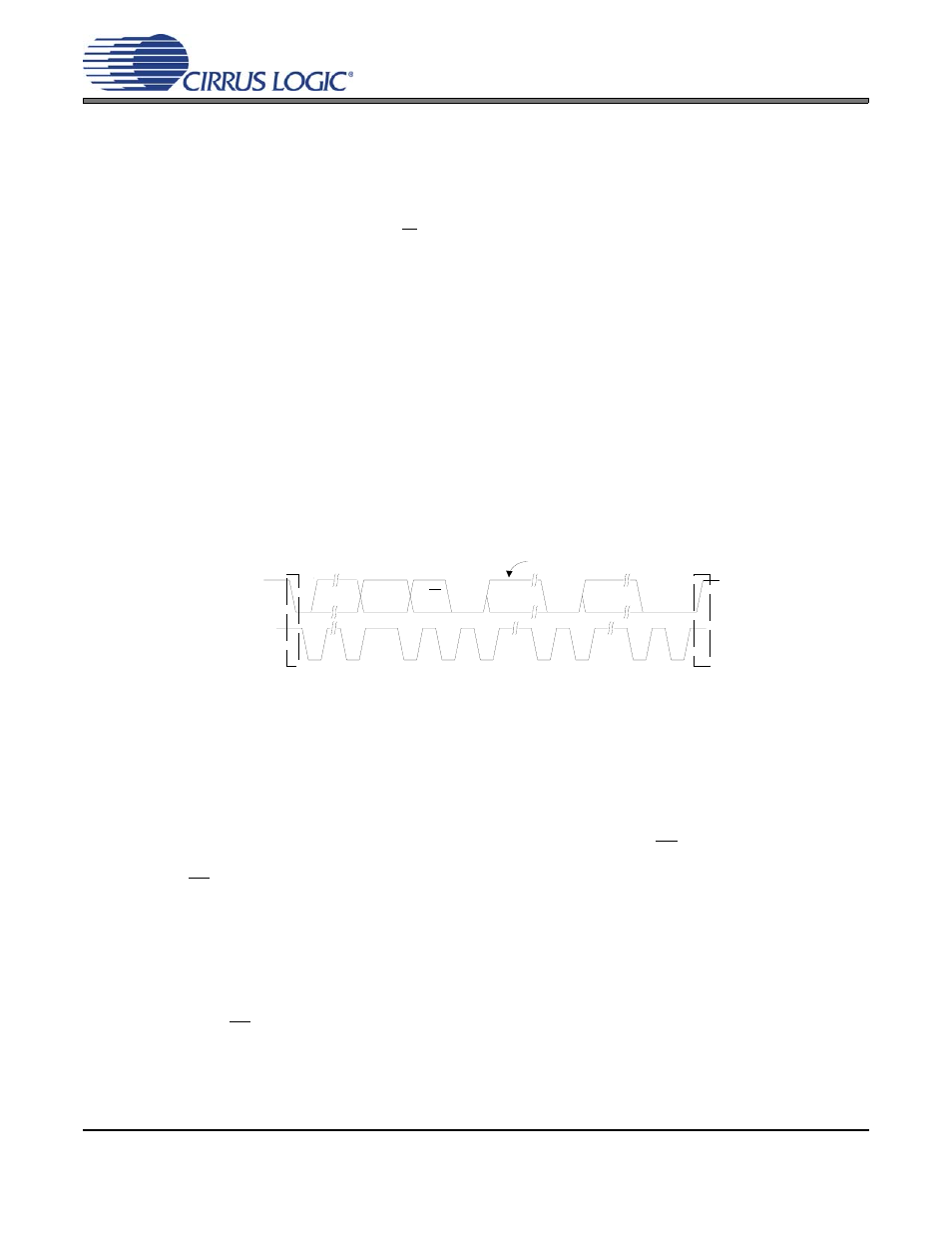
S D A
S C L
100110
AD0
R/W
S ta rt
ACK
DAT A
1-8
A CK
DA TA
1-8
ACK
Stop
NOTE
NOTE: If operation is a write, this byte contains the M em ory Address Pointer, M AP. If
operation is a read, this byte contains the data of the register pointed to by the M AP.
Figure 9. Control Port Timing, I²C Mode