8 control port bit definitions, 9 power-up/reset/power down mode, Cs4228a – Cirrus Logic CS4228A User Manual
Page 19: Figure 15. control port timing, i, C slave mode write, Figure 16. control port timing, i, C slave mode read
CS4228A
19
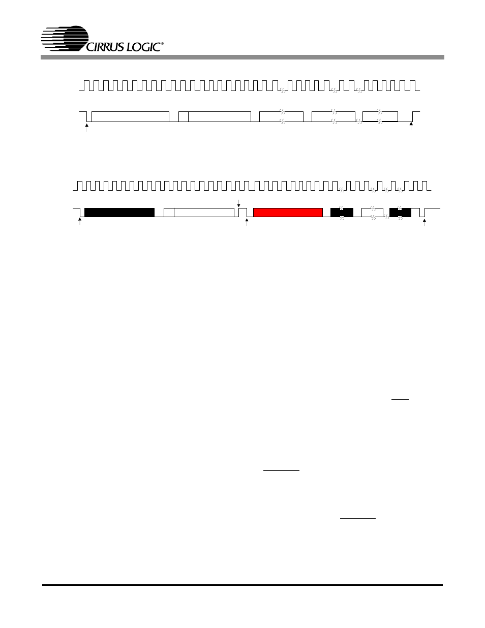
Since the read operation can not set the MAP, an
aborted write operation is used as a preamble. As
shown in Figure 16, the write operation is aborted
after the acknowledge for the MAP byte by sending
a stop condition. The following pseudocode illus-
trates an aborted write operation followed by a read
operation.
Send start condition.
Send 001000x0 chip address & write operation.
Receive acknowledge bit.
Send MAP byte, auto increment off.
Receive acknowledge bit.
Send stop condition, aborting write.
Send start condition.
Send 001000x1 chip address & read operation.
Receive acknowledge bit.
Receive byte, contents of selected register.
Send acknowledge bit.
Send stop condition.
Setting the auto increment bit in the MAP allows
successive reads or writes of consecutive registers.
Each byte is separated by an acknowledge bit.
3.8
Control Port Bit Definitions
All registers are read/write, except the Chip Status
register which is read-only. For more detailed in-
formation, see the bit definition tables.
3.9
Power-up/Reset/Power Down Mode
Upon power up, the user should hold RST = 0 until
the power supplies and clocks stabilize. In this
state, the control registers are reset to their default
settings, and the device remains in a low power
mode in which the control port is inactive. The part
may be held in a low power reset state by clearing
the DIGPDN bit in the Chip Control register. In this
state, the digital portions of the CODEC are in re-
set, but the control port is active and the desired
register settings can be loaded. Normal operation is
achieved by setting the DIGPDN bit to 1, at which
time the CODEC powers up and normal operation
begins.
4
5
6
7
24 25
SCL
CHIP ADDRESS (WRITE)
MAP BYTE
DATA
DATA +1
START
ACK
STOP
ACK
ACK
ACK
0
0
1
0
0
0
AD0 0
SDA
INCR
6
5
4
3
2
1
0
7
6
1
0
7
6
1
0
7
6
1
0
0
1
2
3
8
9
12
16 17 18
19
10 11
13 14 15
27 28
26
DATA +n
Figure 15. Control Port Timing, I
2
C Slave Mode Write
SCL
CHIP ADDRESS (WRITE)
MAP BYTE
DATA
DATA +1
START
ACK
STOP
ACK
ACK
ACK
0
0
1
0
0
0
AD0 0
SDA
0
0
1
0
0
0
AD0 1
CHIP ADDRESS (READ)
START
INCR
6
5
4
3
2
1
0
7
0
7
0
7
0
NO
16
8
9
12 13 14 15
4
5
6
7
0
1
20 21 22 23 24
26 27 28
2
3
10 11
17 18
19
25
ACK
DATA + n
STOP
Figure 16. Control Port Timing, I
2
C Slave Mode Read