Characteristics and specifications, Recommended operating conditions, Absolute maximum ratings – Cirrus Logic CS2300-OTP User Manual
Page 6: Dc electrical characteristics, Cs2300-otp
CS2300-OTP
6
DS844F2
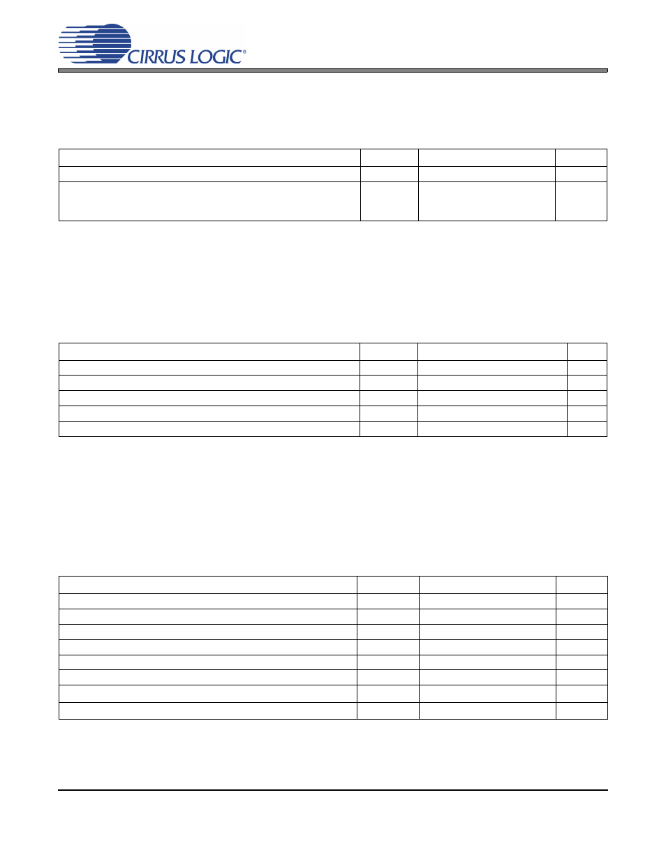
3. CHARACTERISTICS AND SPECIFICATIONS
RECOMMENDED OPERATING CONDITIONS
GND = 0 V; all voltages with respect to ground. (
Notes:
1. Device functionality is not guaranteed or implied outside of these limits. Operation outside of these limits
may adversely affect device reliability.
2. CLK_IN must not be applied when these conditions are not met, including during power up. See
for required power up procedure.
ABSOLUTE MAXIMUM RATINGS
GND = 0 V; all voltages with respect to ground.
WARNING:
Operation at or beyond these limits may result in permanent damage to the device.
Notes:
3. The maximum over/under voltage is limited by the input current except on the power supply pin.
DC ELECTRICAL CHARACTERISTICS
Test Conditions (unless otherwise specified): VD = 3.1 V to 3.5 V; T
A
= -10°C to +70°C (Commercial Grade);
T
A
= -40°C to +85°C (Automotive Grade).
Notes:
4. To calculate the additional current consumption due to loading (per output pin), multiply clock output
frequency by load capacitance and power supply voltage.
For example,
f
CLK_OUT
(49.152 MHz) * C
L
(15 pF) * VD (3.3 V) = 2.4 mA of additional current due to
these loading conditions on CLK_OUT.
Parameters
Symbol Min Typ
Max
Units
DC Power Supply
VD
3.1
3.3
3.5
V
Ambient Operating Temperature (Power Applied)
Commercial Grade
Automotive Grade
T
AC
T
AD
-10
-40
-
-
+70
+85
°C
°C
Parameters
Symbol
Min
Max
Units
DC Power Supply
VD
-0.3
6.0
V
Input Current
I
IN
-
±10
mA
Digital Input Voltage (
V
IN
-0.3
VD + 0.4
V
Ambient Operating Temperature (Power Applied)
T
A
-55
125
°C
Storage Temperature
T
stg
-65
150
°C
Parameters
Symbol
Min
Typ
Max
Units
Power Supply Current - Unloaded
I
D
-
18
23
mA
Power Dissipation - Unloaded
P
D
-
59
76
mW
Input Leakage Current
I
IN
-
-
±10
µA
Input Capacitance
I
C
-
8
-
pF
High-Level Input Voltage
V
IH
70%
-
-
VD
Low-Level Input Voltage
V
IL
-
-
30%
VD
High-Level Output Voltage (I
OH
= -1.2 mA)
V
OH
80%
-
-
VD
Low-Level Output Voltage (I
OH
= 1.2 mA)
V
OL
-
-
20%
VD