Cirrus Logic CS2300-OTP User Manual
Cs2300-otp, Fractional-n clock multiplier with internal lco, Features
Copyright
Cirrus Logic, Inc. 2010
(All Rights Reserved)
Fractional-N Clock Multiplier with Internal LCO
Features
Clock Multiplier / Jitter Reduction
– Generates a Low Jitter 6 - 75 MHz Clock
from a Jittery 50 Hz to 30 MHz Clock
Source
Internal LCO Reference Clock
Highly Accurate PLL Multiplication Factor
– Maximum Error Less Than 1 PPM in High-
Resolution Mode
One-Time Programmability
– Configurable Hardware Control Pins
– Configurable Auxiliary Output
Minimal Board Space Required
– No External Analog Loop-filter
Components
General Description
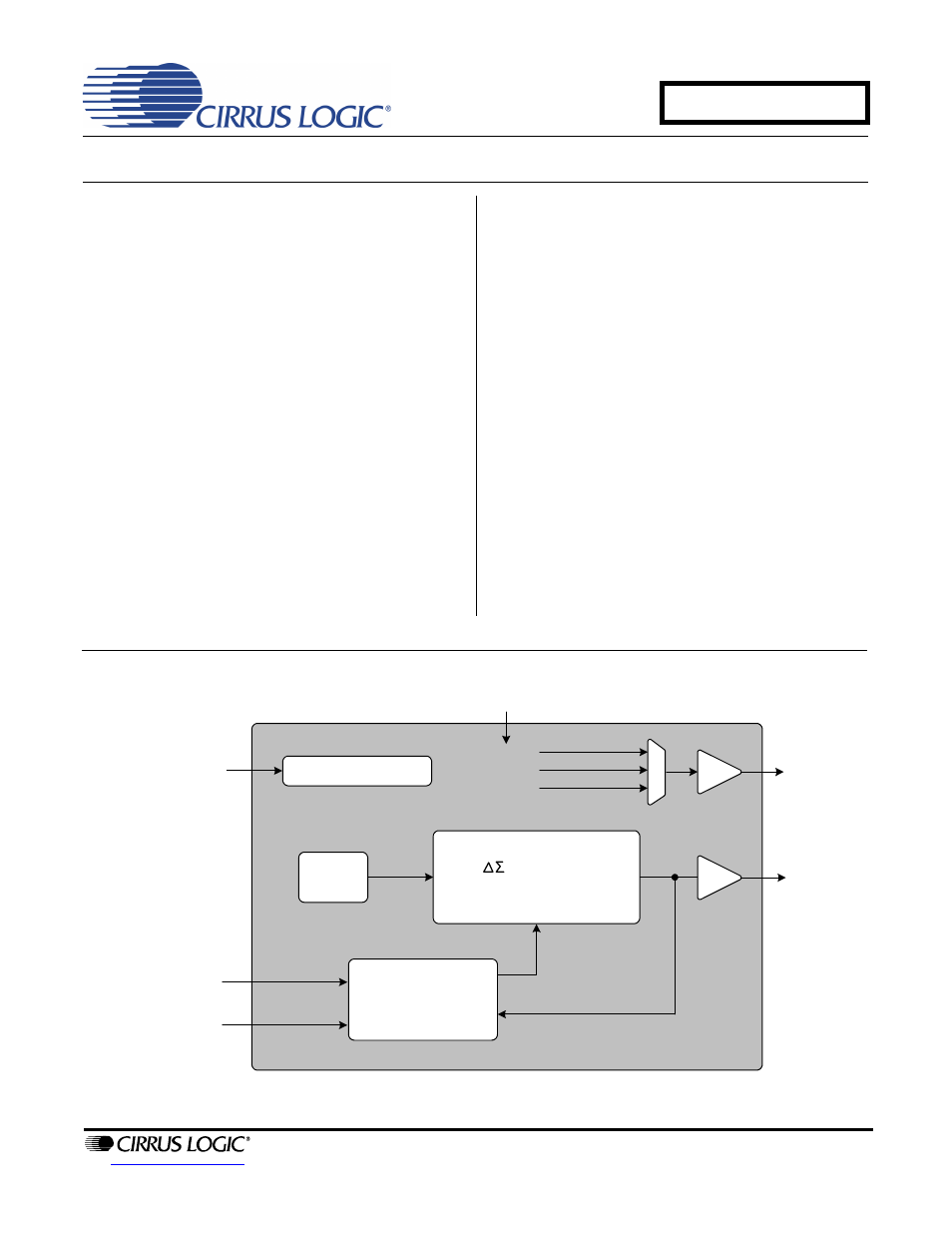
The CS2300-OTP is an extremely versatile system
clocking device that utilizes a programmable phase lock
loop. The CS2300-OTP is based on a hybrid analog-
digital PLL architecture comprised of a unique combina-
tion of a Delta-Sigma Fractional-N Frequency
Synthesizer and a Digital PLL. This architecture allows
for generation of a low-jitter clock relative to an external
noisy synchronization clock with frequencies as low as
50 Hz. The CS2300-OTP has many configuration op-
tions which are set once prior to runtime. At runtime
there are three hardware configuration pins available for
mode and feature selection.
The CS2300-OTP is available in a 10-pin MSOP pack-
age in Commercial (-10°C to +70°C) and Automotive
(-40°C to +85°C) grades. Customer development kits
are also available for custom device prototyping, small
production programming, and device evaluation.
Please see
“Ordering Information” on page 25
plete details.
Auxiliary
Output
6 to 75 MHz
PLL Output
Frequency Reference
3.3 V
Fractional-N
Frequency Synthesizer
Digital PLL & Fractional
N Logic
Output to Input
Clock Ratio
N
PLL Output
Lock Indicator
50 Hz to 30 MHz
Frequency Reference
LCO
Hardware Configuration
Hardware Control
MAY '10
DS844F2
CS2300-OTP
Document Outline
- 1. Pin Description
- 2. Typical Connection Diagram
- 3. Characteristics and Specifications
- 4. Architecture Overview
- 5. Applications
- 5.1 One Time Programmability
- 5.2 Timing Reference Clock
- 5.3 Frequency Reference Clock Input, CLK_IN
- 5.4 Output to Input Frequency Ratio Configuration
- 5.5 PLL Clock Output
- 5.6 Auxiliary Output
- 5.7 Mode Pin Functionality
- 5.8 Clock Output Stability Considerations
- 5.9 Required Power Up Sequencing for Programmed Devices
- 6. Parameter Descriptions
- 7. Calculating the User Defined Ratio
- 8. Programming Information
- 9. Package Dimensions
- 10. Ordering Information