PNI ASIC User Manual
Pni asic, General description, Features
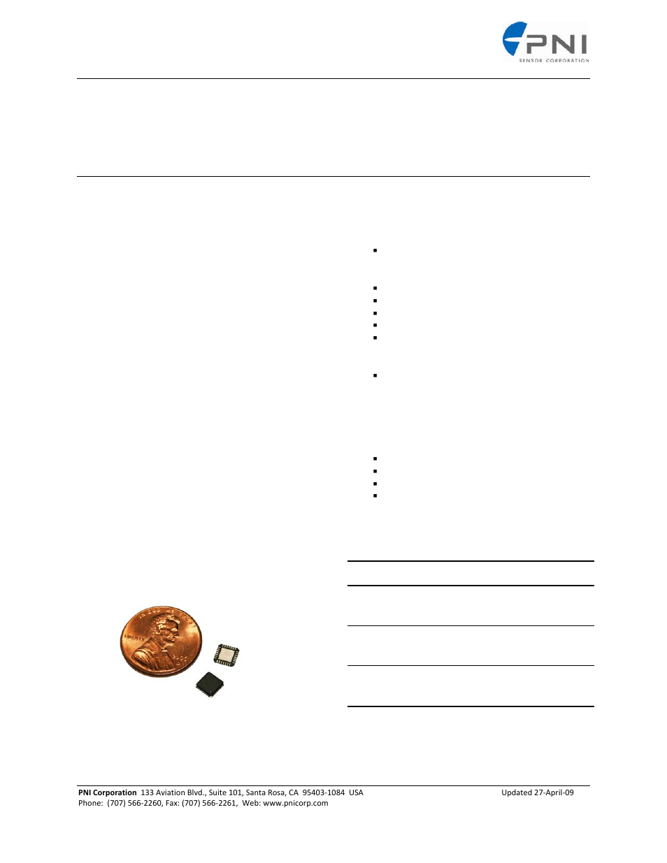
Table of contents
Document Outline
- General Description
- Features
- Applications
- Parameter
- Parameter voltage and current levels
- Vila
- Iilb
- Vol
- Iola
- 5 VDC
- 1
- 26
- VSTBY
- DP
- VDD
- Input protection clamp diode. Connect to VDD
- 2
- 27
- SCLK
- DI
- IBT
- Serial Clock input for SPI port. 1 MHz maximum (Rext = 100 kHz)
- 3
- 28
- MISO
- DO
- OB2
- Serial data output (Master In Slave Out)
- 4
- 1
- MOSI
- DI
- IBA
- Serial data output (Master Out Slave In)
- 5
- 3
- SSNOT
- DI
- IBA
- Active low chip select for SPI port
- ---
- 2
- Not Connected
- 6
- 4
- AVDD
- AP
- VDD
- Supply voltage for analog section
- 7
- 5
- AVSS
- AP
- VSS
- Ground pin for analog section
- 8
- 6
- +ZDRV
- DO
- OB3
- Z sensor drive output
- 9
- 7
- +ZIN
- AI
- AIB
- Z sensor sense input
- 10
- 8
- -ZIN
- AI
- AIB
- Z sensor sense input
- 11
- 9
- -ZDRV
- DO
- OB3
- Z sensor drive output
- 12
- 10
- +YDRV
- DO
- OB3
- Y sensor drive output
- 13
- 11
- +YIN
- AI
- AIB
- Y sensor input
- 14
- 12
- DVDD
- DP
- VDD
- Supply voltage for digital section
- 15
- 13
- -YIN
- AI
- AIB
- Y sensor input
- 16
- 14
- -YDRV
- DO
- OB3
- Y sensor drive output
- 17
- 15
- +XDRV
- DO
- OB3
- X sensor drive output
- 18
- 16
- +XIN
- AI
- AIB
- X sensor sense input
- 19
- 17
- -XIN
- AI
- AIB
- X sensor sense input
- 20
- 18
- -XDRV
- DO
- OB3
- X sensor drive output
- 21
- 19
- DVSS
- DP
- VSS
- Ground pin for digital section
- ---
- 20
- Not connected
- 22
- 21
- COMP
- DO
- OB1
- Comparator output. Used for diagnostics.
- 23
- 22
- RESET
- DI
- IBA
- Rest input
- 24
- 23
- DRDY
- DO
- OB1
- Data ready
- 25
- 24
- DHST
- DIO
- IOIA
- High speed oscillator output. Output is ½ clock speed. Use for diagnostics
- 26
- 25
- REXT
- AI
- AIB
- External timing resistor for high speed clock. 100 k ohm typical
- Exposed Paddle (center Pad)
- Connect to analog ground
- MOSI – Master Out Slave In
- SSNOT – Slave Select
- SCLK – Serial Clock
- MISO – Master In Slave Out
- RESET
- DRDY – Data Ready
- DHST – High Speed Oscillator Test
- PS0, PS1, and PS2 – Period Select
- ODIR – Oscillator Direction
- MOT – Magnetic Oscillator Test
- ASO & ASI – Axis Select
- Function
- AS1
- AS0
- 2 MHz scaling
- 0
- 0
- X axis
- 0
- 1
- Y axis
- 1
- 0
- Z axis
- 1
- 1
- Pad
- Function
- X (mm)
- Y (mm)
- 1
- VSTBY
- –655
- 968
- 2
- SCLK
- –755
- 968
- 3
- MISO
- –893
- 968
- 4
- MOSI
- –1012
- 968
- 5
- SSNOT
- –1128
- 968
- 6
- AVDD
- –1125
- 226
- 7
- AVSS
- –1125
- 62
- 8
- APZDRV
- –1125
- –81
- 9
- APZIN
- –1134
- –966
- 10
- ANZIN
- –1012
- –966
- 11
- ANZDRV
- –893
- –966
- 12
- APYDRV
- –448
- –966
- 13
- APYIN
- –3
- –966
- 14
- DVDD
- 115
- –966
- 15
- ANYIN
- 237
- –966
- 16
- ANYDRV
- 357
- –966
- 17
- APXDRV
- 802
- –966
- 18
- APXIN
- 1118
- –403
- 19
- ANXIN
- 1118
- –312
- 20
- ANXDRV
- 1118
- –189
- 21
- DVSS
- 1118
- 225
- 22
- COMP
- 1126
- 968
- 23
- RESET
- 1008
- 968
- 24
- DRDY
- 887
- 968
- 25
- DHST
- 768
- 968
- 26
- REXT
- 650
- 968
- Reflow Parameter
- Temperature (°C)
- Time (sec)
- Preheat Temperature (TSmin to TSmax)
- 150°C – 200°C
- 60-180
- Temperature TL (typical solder melting point)
- >218°C
- TSmax to TL Ramp-up Rate
- 3°C/second max
- Peak Temperature TP
- 260°C
- Time 25°C to Peak TP
- 6 minute max
- Time Maintained Above Temperature TL (tL)
- 218°C
- 60-120
- Soak (time within 5° of actual Peak TP)
- 10-20
- Ramp-down Rate
- 4°C/second max
- Parameter voltage and current levels
- Parameter