Parameter, Specifications – PNI ASIC User Manual
Page 2
PNI ASIC
Specifications
SPECIFICATIONS
C A U T I O N :
Stresses beyond those listed under Table 2 may cause permanent damage to the device. These are
stress ratings only. Functional operation of the device at these or any other conditions beyond
those indicated in the operational sections of the specifications is not implied. Exposure to
absolute maximum rating conditions for extended periods may affect device reliability
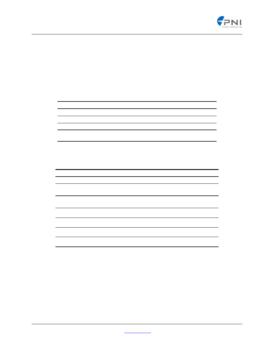
Table 2: Absolute Maximum Ratings
Symbol
Parameter Minimum
Maximum
V
DD
DC supply voltage
-0.3 VDC
5.25 VDC
V
IN
Input pin voltage
V
DD
-0.3 VDC
V
DD
+ 0.3 VDC
I
IN
Input pin current
-10mA at 25° C
10mA at 25° C
T
STRG
Storage
Temperature
-40°C
125°C
Table 3: Supply Operating Conditions
Symbol Parameter
Minimum
Maximum
V
DD
Digital DC Supply
2.2 VDC
5.0 VDC
I
DD
(nominal)
Idle
(V
DD
= 3 VDC)
1
µA
I
DD
(maximum)
Operating
(V
DD
= 3 V, SEN-S65)
0.5
mA
ILKSTBY
a
I
DD
@ VSTBY pin
100
nA
V
SS
Digital Ground
0 V
0V
TA Ambient
Temperature
-20°C
70°C
ESD Rating
± 2 KV at 200 pF
a.
VSTBY = 5.5V, AV
DD
= DV
DD
= AV
SS
= DV
SS
= 0 V, Temperature 27 × C
PNI Corporation 133 Aviation Blvd., Suite 101, Santa Rosa, CA 95403‐1084 USA;, Fax: (707) 566‐2261
For the most current specifications, please visit our website at:
www.pnicorp.com
‐ 2 ‐