2 back panel pcb, Figure 4 back panel pcb, Figure 4 – Kaman KDM-8206 User Manual
Page 8
Kaman Precision Products
PART NO: 860515-001
www.kamansensors.com
Last Revised: 6/20/2011
8
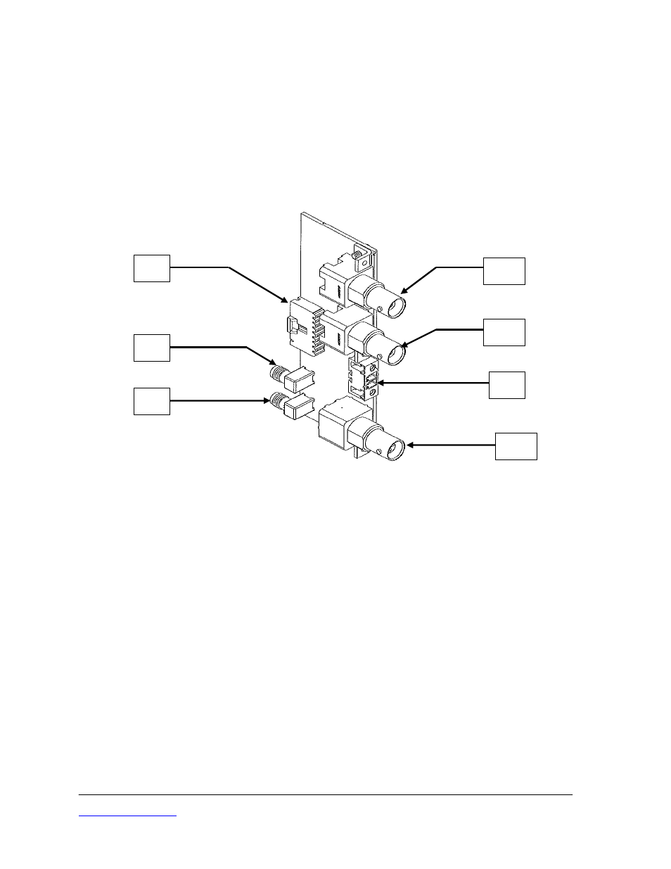
3.2 Back Panel PCB
The Back Panel PCB is installed in the rack just as its name indicates, to the rear panel
of the rack or instrument enclosure. It is secured to the rear panel with three flat head
screws and with the BNC connector nuts. A Back Panel PCB is required for each
Measuring Channel installed in the rack. Its purpose is to provide external I/O
connections for each Measuring Channel and transmit them to the Back Plane PCB.
Figure 4
Back Panel PCB
Connections to the Back Panel are:
BNC1 Coaxial V+ connector for single ended and differential voltage output.
BNC2 Coaxial V- connector for differential voltage output option. Not installed if
this option is not requested.
JA Sensor connection to Back Plane PCB for a single coil sensor. Sensor active
coil for a dual coil sensor.
JB Sensor inactive coil connection to Back Plane PCB for a dual coil sensor.
Not connected for a single coil sensor.
P1 Ribbon cable connector to Back Plane PCB
SEN Twin BNC sensor connector.
TB1 Two position terminal block for 4-20 mA current output.
JB
JA
P1
SEN
TB1
BNC2
BNC1