Figure 11. output alarm circuit optically isolated, Output alarm circuit optically isolated, Pf power failure optocoupler timing diagram – KEPCO HSF 600W Series (suffix M and MZ) Operator Manuals User Manual
Page 16
14
HSF (M) 600W 022713
FIGURE 10. DIP SWITCH SETTINGS FOR OPTICALLY COUPLED LOGICAL ALARM
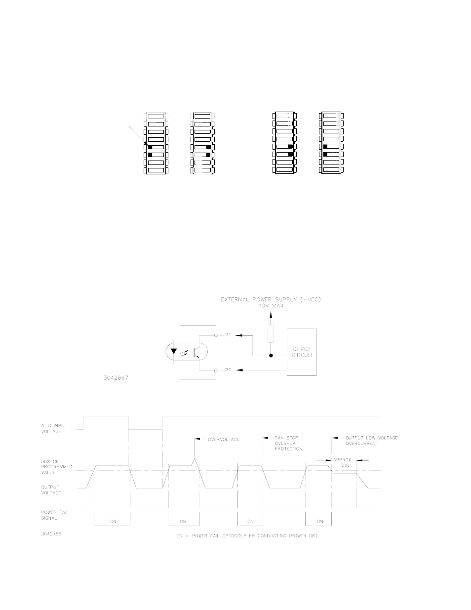
The logic alarm circuit is a diode transistor optical coupler (see Figure 11). The transistor is nor-
mally conducting. When the alarm is activated upon detection of power loss, overvoltage, fan
fault, overtemperature or overcurrent condition, the transistor cuts off and the collector emitter cir-
cuit is open. Figure 12 is a timing diagram of the power fail signal.
The default state of the alarm is logic low. The sink current for the optocoupler is 50mA maximum,
the maximum collector to emitter saturation voltage is 0.40 Volts, and the collector to emitter volt-
age is 40 volts maximum. The PF signals are isolated from the AC input and DC output.
FIGURE 11. OUTPUT ALARM CIRCUIT OPTICALLY ISOLATED
FIGURE 12. ±PF POWER FAILURE OPTOCOUPLER TIMING DIAGRAM
3042878
5
5 +PF
+PF 5
5
SW1
-PF 6
6
SW2
6
6 -PF
OFF
ON
OFF
ON
USE N.O. AND N.C CONTACTS
(FACTORY DEFAULT)
OF INTERNAL RELAY
A
LOGICAL ALARM
USE OPTICALLY-COUPLED
B
(+PF AND -PF)
5
6
6
SW1
5
SW2
OFF
ON
ON
OFF
+PF 5
-PF 6
6 -PF
5 +PF
TAB