Qphy-lpddr2 software option – Teledyne LeCroy QPHY-LPDDR2 User Manual
Page 9
QPHY-LPDDR2 Software Option
QPHY-LPDDR2-OM-G Rev B
9
BL/2 + 1 - WL clock cycles. Note that if a read burst is truncated with a Burst Terminate (BST) command,
the effective burst length of the truncated read burst should be used as “BL” to calculate the minimum
read to write delay.
Burst Write
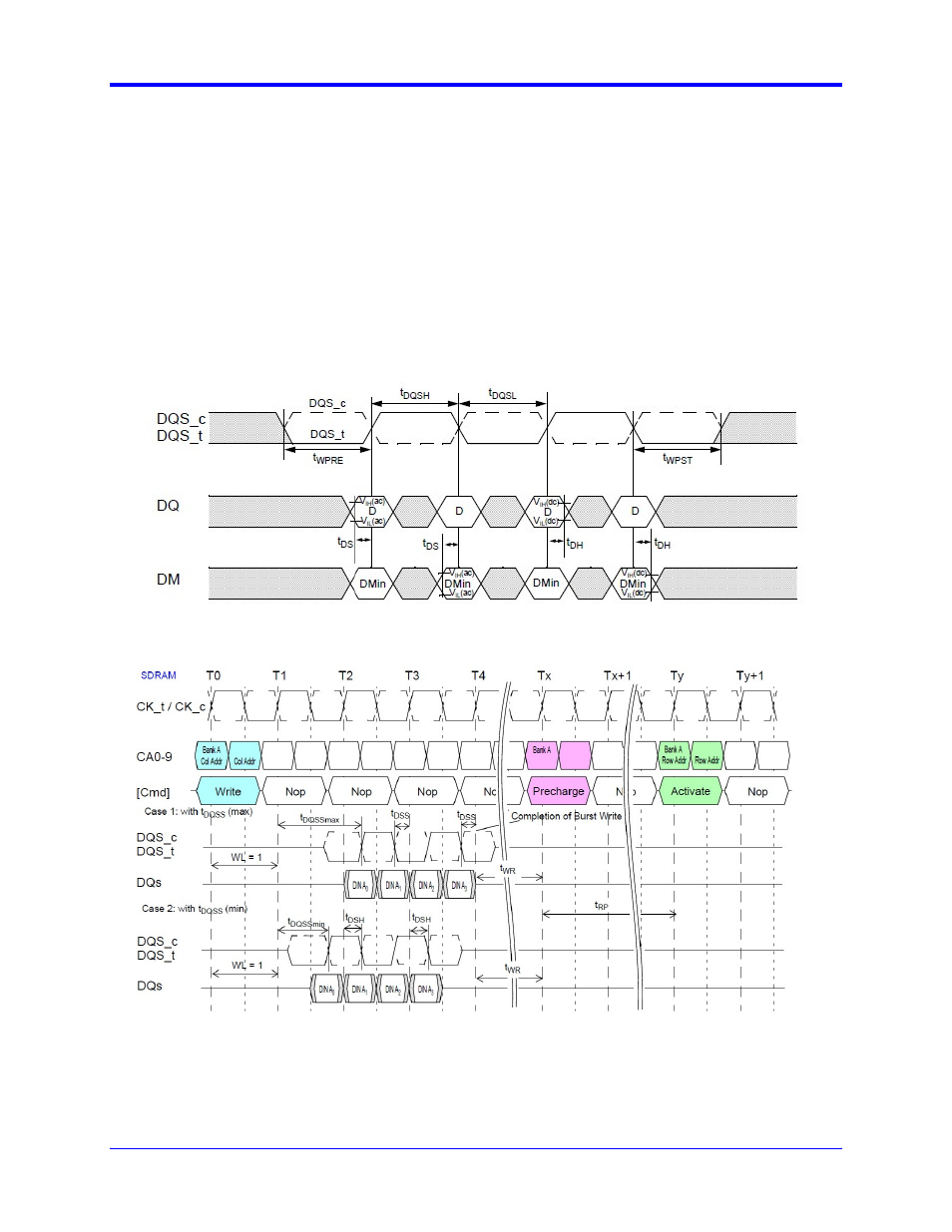
The Burst Write command is initiated by having CS_n LOW, CA0 HIGH, CA1 LOW and CA2 LOW at the
rising edge of the clock. The command address bus inputs, CA5r-CA6r and CA1f-CA9f, determine the
starting column address for the burst. The Write Latency (WL) is defined from the rising edge of the clock
on which the Write Command is issued to the rising edge of the clock from which the tDQSS delay is
measured. The first valid datum shall be driven WL * tCK + tDQSS from the rising edge of the clock from
which the Write command is issued. The data strobe signal (DQS) should be driven LOW tWPRE prior to
the data input. The data bits of the burst cycle must be applied to the DQ pins tDS prior to the respective
edge of the DQS and held valid until tDH after that edge. The burst data are sampled on successive
edges of the DQS until the burst length is completed, which is 4, 8, or 16 bit burst.
Figure 3. Data input (write) timing [JESD209-2D figure 40]
Figure 4. Burst write: WL = 1, BL = 4 [JESD209-2D figure 41]