Teledyne LeCroy QPHY-LPDDR2 User Manual
Page 8
8
QPHY-LPDDR2-OM-G Rev B
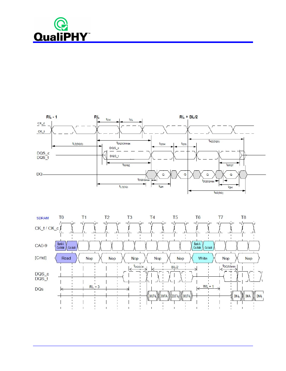
Burst Read
The Burst Read command is initiated by having CS_n LOW, CA0 HIGH, CA1 LOW and CA2 HIGH at the
rising edge of the clock. The command address bus inputs, CA5r-CA6r and CA1f-CA9f, determine the
starting column address for the burst. The Read Latency (RL) is defined from the rising edge of the clock
on which the Read Command is issued to the rising edge of the clock from which the tDQSCK delay is
measured. The first valid datum is available RL * tCK + tDQSCK + tDQSQ after the rising edge of the
clock where the Read Command is issued. The data strobe output is driven LOW tRPRE before the first
rising valid strobe edge. The first bit of the burst is synchronized with the first rising edge of the data
strobe. Each subsequent data-out appears on each DQ pin edge aligned with the data strobe. The RL is
programmed in the mode registers.
Figure 1. Data output (read) timing [JESD209-2D figure 23]
Figure 2. Burst read followed by burst write [JESD209-2D figure 32]
The minimum time from the burst read command to the burst write command is defined by the Read
Latency (RL) and the Burst Length (BL). Minimum read to write latency is RL + RU(tDQSCKmax/tCK) +