Ronan X11SN User Manual
Page 9

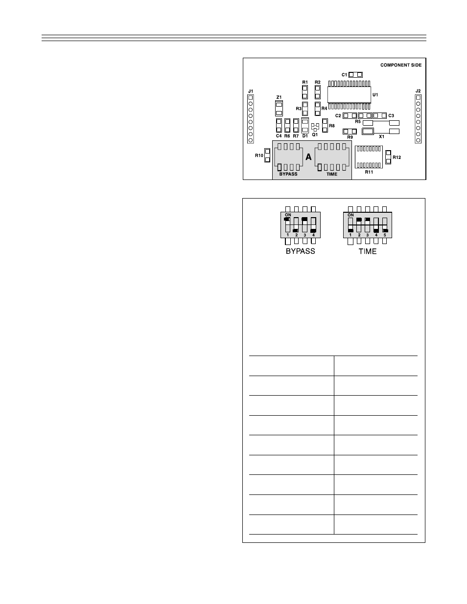
Bypass Switch Selection
Channel A(1) and Channel C(3) in ON position by-
passes the time selected by TIME. The FC response
for Channel A and Channel C will be 20 ms. nominal.
Channel B(2) and Channel D(4) in off position selects
the field contact response selected by TIME, in this
case, 3.0 seconds.
Time Switch Selection
The table below shows that with switches 2 and 3 in
the ON position and 1, 4, and 5 in the OFF position,
3.0 seconds is selected for field contact response.
Detail A: Time Board Operation Example.
the field contact response will be the time
selected by switch TIME. See Figure 2, Detail
A for a time board operation example.
Dual horn selection is offered as an option to
choose the active horn bus HORN1 and
HORN2. This option should be used when the
user needs to separate module groups by
activating different horns. On PCBs X11-
1013C and X11-1020, the horn selection is
made at headers HORNA-HORND. These
refer to associated field contacts FCA-FCD.
The programmable version uses a slide switch
labeled HORN. The OFF position selects
HORN1 and the ON position selects HORN2.
Switches 1-4 are connected for field contacts
FCA-FCD respectively.
Although ordering auxiliary relay boards is not
mandatory, the X11SN system is designed so
that auxiliary relay behavior must be selected.
The basic options available choose between
Normally Energized/Deenergized following the
field contact or alarm cycle behavior. The spe-
cific options available can be consulted in the
X11SN sales brochure. When selectable auxil-
iary behavior is chosen, an on board selector
switch is located at SW1 on PCBs X11-1013C
and X11-1020. PCB X11-1019B uses selector
switch AUX. See specific sequence charts for
specific auxiliary relay behavior. NOTE:
Unless otherwise specified, the standard auxil-
iary relay option is normally non-energized fol-
low field contact.
PCB X11-1019B (programmable) has an addi-
tional header J7 and slideswitch GEN. The
header J7 is used for parallel port program-
ming of the device located at U6. This header
should remain unconnected and without any
additional connected shunts during normal cir-
cuit operation. The slideswitch GEN is provid-
ed when unusual or non-standard circuit per-
formance or configuration is necessary.
Normally, most assemblies do not populate
slideswitch GEN. See Figure 3 (see page 9),
Details B and C for header and switch loca-
tions of PCB X11-1019B.
The combination display/alarm module con-
tains a single, dual, triple, or quad alarm chan-
nel circuit with the appropriate lamp display
constructed as a single plug-in module. The
modules are removable from the front of the
system without the interference to the remain-
ing channels of the
8
Figure 2: X11-1024 PCB Switch Locations.
Switch Time
Time
Switch Time
Time
1 2 3 4 5
Delay
1 2 3 4 5
Delay
00000
50 msec.
00001
45 sec.
10000
100 msec.
10001
1 min.
01000
300 msec.
01001
90 sec.
11000
0.5 sec.
11001
2 min.
00100
1.0 sec.
00101
3 min.
10100
2.0 sec.
10101
4 min.
01100
3.0 sec.
01101
5 min.
11100
4.0 sec.
11101
6 min.
00010
5.0 sec.
00011
7 min.
10010
6.0 sec.
10011
8 min.
01010
7.0 sec.
01011
9 min.
11010
8.0 sec.
11011
10 min.
00110
9.0 sec.
00111
15 min.
10110
10.0 sec.
10111
30 min.
01110
15.0 sec.
01111
45 min.
11110
30.0 sec.
11111
60 min.
