Connection diagrams, Pin descriptions – Atec Superior-Electric-L116b User Manual
Page 2

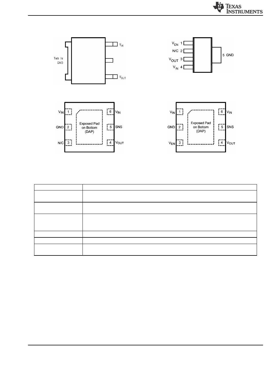
Connection Diagrams
20126603
TO-252, Top View
LP38690DT-X.X
20126604
SOT-223, Top View
LP38692MP-X.X
20126605
6-Lead LLP, Top View
LP38690SD-X.X
20126606
6-Lead LLP, Top View
LP38692SD-X.X
Pin Descriptions
Pin
Description
V
IN
This is the input supply voltage to the regulator. For LLP devices, both V
IN
pins must be tied together
for full current operation (500mA maximum per pin).
GND
Circuit ground for the regulator. For the TO-252 and SOT-223 packages this is thermally connected
to the die and functions as a heat sink when the soldered down to a large copper plane.
SNS
Output sense pin allows remote sensing at the load which will eliminate the error in output voltage
due to voltage drops caused by the resistance in the traces between the regulator and the load. This
pin must be tied to V
OUT
.
V
EN
The enable pin allows the part to be turned ON and OFF by pulling this pin high or low.
V
OUT
Regulated output voltage.
DAP
LLP Only - The DAP (Exposed Pad) functions as a thermal connection when soldered to a copper
plane. See
section in
for more information.
LP38690
LP38692
2
Copyright © 1999-2012, Texas Instruments Incorporated
