Atec Tektronix-TDS-5052-5054-5104 User Manual
Page 4

Trigger Modes
Edge – Positive or negative slope on any channel or
front panel auxiliary input. Coupling includes DC, AC,
noise reject, HF reject and LF reject.
Video – Trigger on NTSC, PAL, SECAM, analog HDTV
and non-standard video formats.
Glitch – Trigger on or reject glitches of positive,
negative or either polarity. Minimum glitch width is
1.0 ns with 200 ps resolution.
Width – Trigger on width of positive or negative
pulse either within or out of selectable time limits
(1 ns to 1 s).
Runt – Trigger on a pulse that crosses one threshold
but fails to cross a second threshold before crossing
the first again. Event can be time or logic qualified
(logic on 4 channel models only).
Window – Trigger on an event that enters or exits a
window defined by two user-adjustable thresholds.
Event can be time or logic qualified (logic on 4
channel models only).
Timeout – Trigger on an event which remains high,
low or either, for a specified time period, selectable
from 1 ns to 1 s with 200 ps resolution.
Digital Phosphor Oscilloscopes
TDS5000 Series
Digital Phosphor Oscilloscopes • TDS5000 Series • www.tektronix.com/tds5000
4
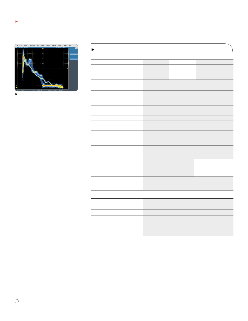
Display of a current vs. voltage trajectory
XY plot of the DUT. This highly dynamic
waveform display provides continuous
coverage of device performance – the
waveform data is continuously streamed
to the display. Color-grading reveals the
distribution of signal activity for comparison
against device Safe Operating Area
(SOA) characteristics.
Vertical System
TDS5052
TDS5054
TDS5104
Input Channels
2
4
4
Analog Bandwidth (–3 dB)
500 MHz
500 MHz
1 GHz
5 mV/div to 1 V/div
Calculated Rise Time 5 mV/div (typical)
800 ps
800 ps
400 ps
Hardware Bandwidth Limits
150 MHz or 20 MHz
Input Coupling
AC, DC, GND
Input Impedance
1 M
Ω
±1% or 50
Ω
±1%
Input Sensitivity,
1 mV/div to 10 V/div
1 M
Ω
Input Sensitivity,
1 mV/div to 1 V/div
50
Ω
Vertical Resolution
8-bits (>11-bits w/ averaging)
Max Input Voltage,
±150 V CAT I derate at 20 dB/decade to 9 V
RMS
above 200 kHz
1 M
Ω
Max Input Voltage,
5 V
RMS
with peaks <±30 V
50
Ω
DC Gain Accuracy
1.5% with offset set to 0 V
Offset Range, 1 M
Ω
1 mV/div to 99.5 mV/div ±1 V
100 mV/div to 1 V/div ±10 V
1.01 V/div to 10 V/div ±100 V
Offset Range, 50
Ω
1 mV/div to 99.5 mV/div ±1 V
1 mV to 50 mV/div ±0.5 V
100 mV/div to1 V/div ±10 V
50.5 mV to 99.5 mV ±0.25 V
100 mV to 500 mV ±5 V
505 mV to 1 V/div ±2.5 V
Channel-to-channel Isolation
≥
100:1 at
≤
100 MHz and
≥
30:1 at >100 MHz
Any Two Channels at
up to the rated bandwidth
Equal Vertical Scale
Timebase System
Timebase Range
200 ps/div to 40 s/div
Timebase Delay Time Range
16 ns to 250 s
Channel-to-channel Deskew Range
±25 ns
Delta Time Measurement Accuracy
±(0.30 sample interval) + (15 ppm * reading)
Trigger Jitter (RMS)
8 ps
RMS
(typical)
Long Term Sample Rate
±15 ppm over
≥
1 ms interval
and Delay Time Accuracy
Characteristics
