Atec Tektronix-DTG5334 User Manual
Page 5
Data Timing Generator — DTG5078 • DTG5274 • DTG5334
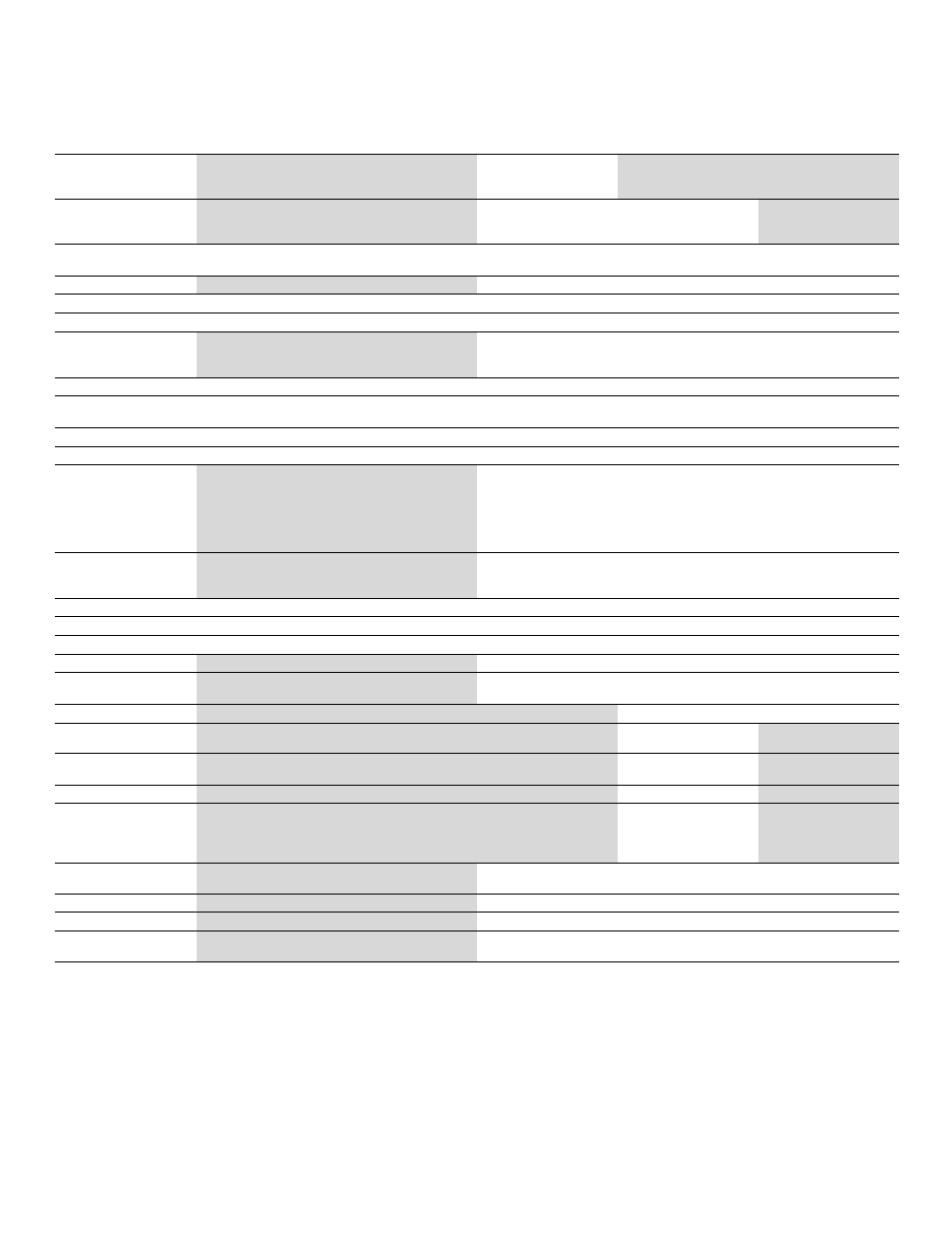
Output Module Characteristics
Basic Features
DTGM21
DTGM30
DTGM31
DTGM32
Output Channels and
Connections
4 single-ended (installed in DTG5078)
2 single-ended (DTG5274/5334)
4 SMA connectors
2 complementary channels
4 SMA connectors
1 complementary channel
2 SMA connectors
Maximum Data Rate
(calculated by transition
time)
1.1 Gb/s
3.35 Gb/s
350 Mb/s*
2
Normal/ Complement
(Invert)
Selectable
Source Impedance
50 Ω / 23 Ω (selectable)
50 Ω
Enable/Disable
Yes (software switch)
Output Channel Timing
Transition Times (20 - 80%)
(50 Ω )
<340 ps (VOL = 0.0, VOH = 1.0) (typical)
<1.0 ns (VOL = -1.65, VOH = 3.7) (typical)
<95 ps (VOL = 0.0, VOH = 0.1) (typical)
<110 ps (VOL = 0.0, VOH = 1.0) (typical)
Transition Time Control
No
Slew Rate Control
Range
–
Setting Resolution
–
Channel Output Levels
Amplitude/Resolution
0.25 to 5.35 V
p-p
/ 5 mV (from 23 Ω source
impedance into 50 Ω)
0.25 to 3.9 V
p-p
/ 5 mV (from 50 Ω source
impedance into 50 Ω)
0.50 to 7.8 V
p-p
/ 5 mV (from 50 Ω source
impedance into 1 MΩ)
0.03 to 1.25 V
p-p
/ 5 mV (into 50 Ω )*
3
0.06 to 2.5 V
p-p
/ 5 mV (into 1 MΩ )*
3
Output Voltage Window
-1.65 V to 3.70 V (from 23 Ω source impedance into 50 Ω)
-1.2 V to 2.7 V (from 50 Ω source impedance into 50 Ω)
-2.4 V to 5.4 V (from 50 Ω source impedance into 1 MΩ)
-2.0 V to 2.47 V (into 50 Ω )
-2.0 V to 7.0 V (into 1 MΩ )
DC Accuracy
(±3% of the set value) ±50 mV into 50 Ω to GND
Limit setting
High- and low-level limits can be set
Maximum Output Current
±80 mA
Overshoot
<15% (typical) at High = 1.0 V, Low = 0 V
<10% (typical) at High = 1.0 V, Low = 0 V
Typical Support Native
Logic
TTL, CMOS, (P)ECL, LVPECL
LVDS, CMOS, (P)ECL, LVPECL, CML
External Jitter Control
No
Yes
External Jitter control input
channels and connectors
–
1 single-ended channel
1 SMA connector
2 single-ended channels
2 SMA connectors
Input range
–
-0.5 V to +0.5 V (typical)
Max input: -1.0 V to +1.0 V
-0.5 V to +0.5 V
Jitter Frequency
–
DC to 250 MHz *
4
DC to 50 MHz
Jitter Amplitude
–
240 ps
p-p
for 1 V
p-p
input at
Data rate ≤2.7 Gb/s*
5
Range 1:
Up to 1 ns at 1 V
p-p
Range 2:
Up to 2 ns at 1 V
p-p
External Tri-state (Hi Z)
Control
Yes (SMB input connector)
No
Tri-state Enable
Enable: Hi 3.3 V, Disable Lo: 0.0 V
–
Control Channels
By output module level
–
Delay Time from Inhibit In to
Data Output
Active to Inhibit: 13 ns,
Inhibit to Active: 12 ns
–
*
2
Minimum pulse width >2.86 ns.
*
3
Maximum output amplitude is dependent on output voltage window (offset). (See Figure 1.)
*
4
Up to 400 MHz by overdriving jitter input (max -1.0 V to +1.0 V
p-p
). (See Figure 2.)
*
5
Jitter amplitude at data rates >2.7 Gb/s calculated as {240 - 61.5 × (data rate - 2.7)} ps
p-p
for 1 V
p-p
input (see Figure 3).
www.tektronix.com
5