Functional block diagram, Absolute maximum ratings, Recommended operating conditions – Diodes PAM8908 User Manual
Page 3: Thermal information
PAM8901 / PAM8908
Document number: DSxxxxx Rev. 1 - 1
3 of 12
www.diodes.com
December 2012
© Diodes Incorporated
PAM8901 / PAM8908
A Product Line of
Diodes Incorporated
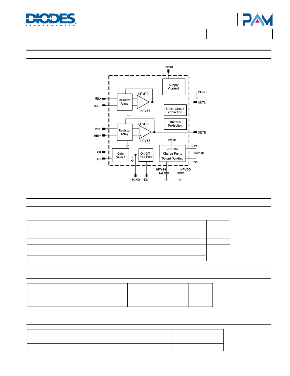
Functional Block Diagram
Absolute Maximum Ratings
(@T
A
= +25°C, unless otherwise specified.)
These are stress ratings only and functional operation is not implied. Exposure to absolute maximum ratings for prolonged time periods may
affect device reliability. All voltages are with respect to ground.
Parameter Rating
Unit
Supply Voltage (PV
DD
)
6.0 V
Input Voltage (INR+, INR-, INL+, INL-)
HPV
SS
-0.3 to HPV
DD
+0.3
V
Control Interface Voltage (G0, G1, EN)
-0.3 to PV
DD
+0.3
V
Storage Temperature
-65 to +150
°C
Maximum Junction Temperature
150
Soldering Temperature
250, 10sec
Recommended Operating Conditions
(@T
A
= +25°C, unless otherwise specified.)
Parameter Rating
Unit
Supply Voltage Range
2.5 to 5.5
V
Ambient Temperature Range
-40 to +85
°C
Junction Temperature Range
-40 to +125
Thermal Information
Parameter Symbol
Package
Max
Unit
Thermal Resistance (Junction to Ambient)
θ
JA
TQFN3x3-16 35 °C/W
Thermal Resisitance (Junction to Case)
θ
JC
TQFN3x3-16 14 °C/W