Typical applications circuit, Pin descriptions – Diodes PAM8908 User Manual
Page 2
PAM8901 / PAM8908
Document number: DSxxxxx Rev. 1 - 1
2 of 12
www.diodes.com
December 2012
© Diodes Incorporated
PAM8901 / PAM8908
A Product Line of
Diodes Incorporated
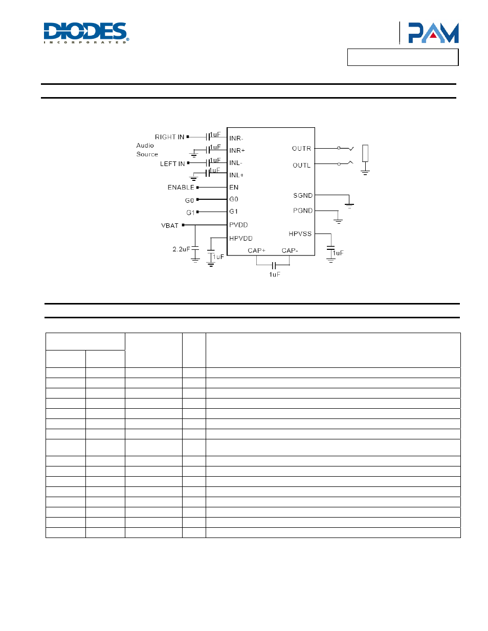
Typical Applications Circuit
(cont.)
Typical Applcation Configuration with Single-Ended Input Signal
Pin Descriptions
Pin Number
T-QFN3x3-16L
Pin Name
I/O/P
Function
PAM8901 PAM8908
1
1 INL-
I
Inverting left input for differential signals.
2
2 INL+
I
Non-inverting left input for differential signals.
3
3 INR+
I
Inverting right input for differential signals.
4
4 INR-
I
Non-inverting right input for differential signals.
5
6 G0
I
Gain select bit 0
6 7 G1 I
Gain select bit 1
7
5 OUTR
O
Right headphone amplifier output. Connect to right terminal of headphone jack.
8 8 HPVSS
P
Charge pump output and negative power supply for output amplifiers; connect 1µF
capacitor to GND
9 10 PGND
P
Power Ground
10 9 CAP-
O
Charge pump negative flying cap.
11 11 CAP+ O
Charge pump positive flying cap.
12 14 PVDD P
Power V
DD
.
13 12 HPVDD
O
Positive power supply for headphone amplifiers. Charge pump positive half V
DD
output.
14 16 OUTL O
Left headphone ampli fier output. Connect to left terminal of headphone jack.
15 15 SGND I
Amplifier reference voltage.
16 13
EN I
Amplifier enabled. Connect to logic low to shutdown; connect to logic high to activate
PAM8901/
PAM8908