Pam3110, Typical applications circuit, Pin configuration and description – Diodes PAM3110 User Manual
Page 2: Functional block diagram
PAM3110
Document number: DSxxxxx Rev. 2 - 2
2 of 13
September 2013
© Diodes Incorporated
PAM3110
A Product Line of
Diodes Incorporated
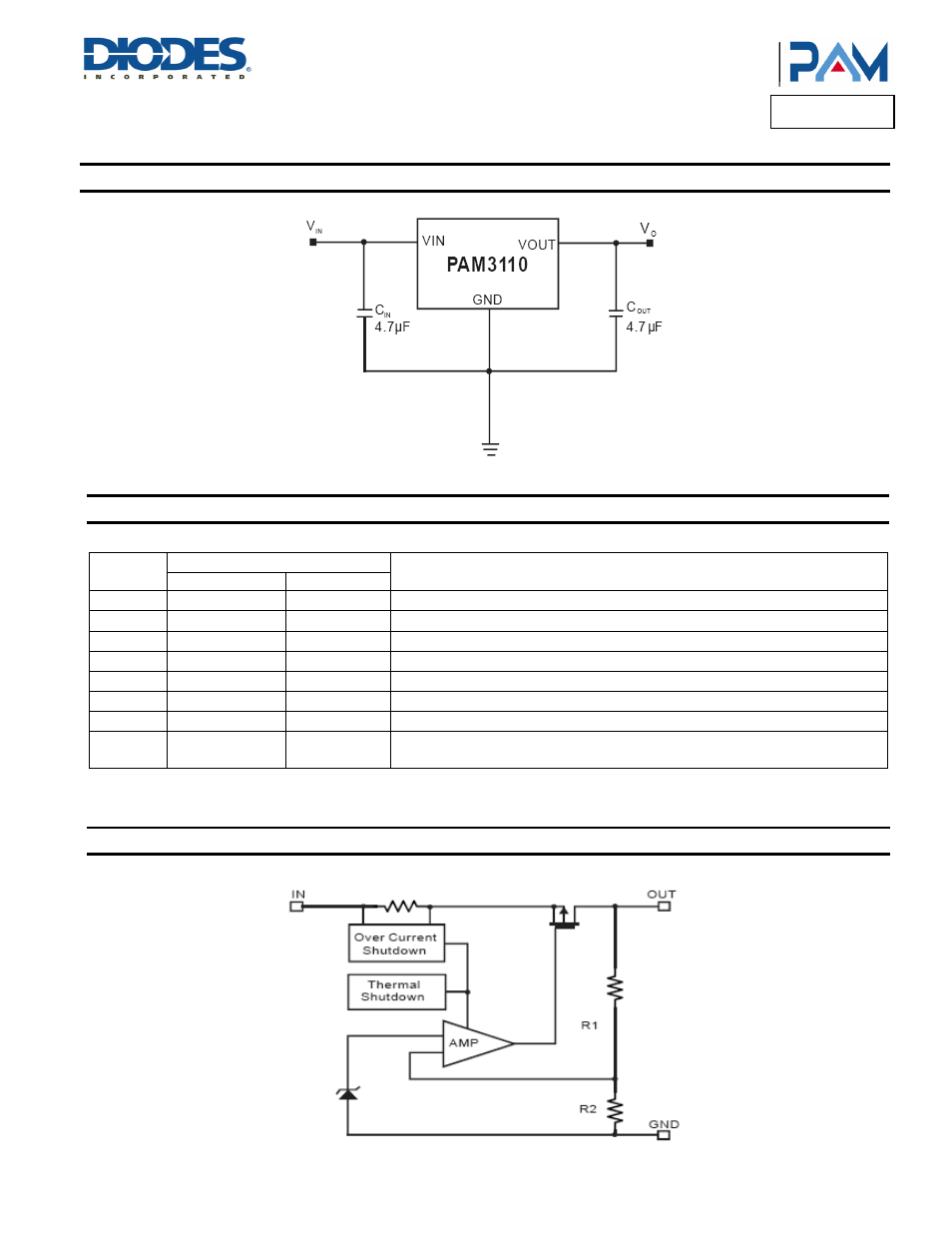
Typical Applications Circuit
Pin Configuration and Description
Pin Name
Pin Number
Function
SOP-8(EP) W-DFN3x3-10
VIN 3
7, 8, 9
Supply Input Voltage.
EN 2
6
Chip Enable (Active-High).
CTRL 4
10
Supply Voltage of ControlCircuitry.
POK 1
5
Power Good Open Drain Output.
ADJ 7
4
Set the output voltage by the feedback resistors. V
O
= 0.8V x (R1 + R2)/R2.
VOUT 6
1, 2, 3
Output Voltage.
NC
5
—
No Internal Connection.
GND
8,
Exposed Pad (9)
Exposed Pad
(11)
Ground. The exposed pad must be soldered to a large PCB and connected to GND
formaximum powe r dissipation.
Functional Block Diagram
See also other documents in the category Diodes Hardware:
- PDS3200 (5 pages)
- PDS340 (5 pages)
- PDS340Q (5 pages)
- PDS360 (5 pages)
- PDS360Q (5 pages)
- PDS4150 (4 pages)
- PDS3100Q (5 pages)
- PDS3100 (5 pages)
- PDS1240CTL (5 pages)
- PDS1045 (5 pages)
- PDS1040L (5 pages)
- PDS1040CTL (5 pages)
- PDS1040 (5 pages)
- PD3S230L (5 pages)
- PD3S230H (3 pages)
- PDS5100Q (5 pages)
- PDS835L (5 pages)
- PDS760 (5 pages)
- PDS560 (5 pages)
- PDS540 (5 pages)
- PDS5100H (5 pages)
- PDS5100 (5 pages)
- PDS4200H (6 pages)
- SBL3060CTP (4 pages)
- SBL30L30CT (3 pages)
- SBL3045CTP (4 pages)
- SBL3040CTP (4 pages)
- SBL2060CTP (4 pages)
- SBL2030CT - SBL2060CT (3 pages)
- SBL2045CTP (4 pages)
- SBL1060CTP (4 pages)
- SBL1040CTP (4 pages)
- SBG3030CT - SBG3045CT (5 pages)
- SB520 - SB560 (3 pages)
- SB370 - SB3100 (3 pages)
- SB320 - SB360 (3 pages)
- SBR10U100CT (5 pages)
- SBR10U150CT (5 pages)
- SBR10A45SP5 (5 pages)
- SBR1060CT (5 pages)
- SBR1045SP5 (5 pages)
- SBR1045SD1 (4 pages)
- SBR1045D1 (5 pages)
- SBR1045CTL (4 pages)
- SBR1040CT (5 pages)