New prod uc t nis5132 electrical characteristics – Diodes NIS5132 User Manual
Page 5
NIS5132
Document number: DS36457 Rev. 1 - 5
5 of 11
December 2013
© Diodes Incorporated
NEW PROD
UC
T
NIS5132
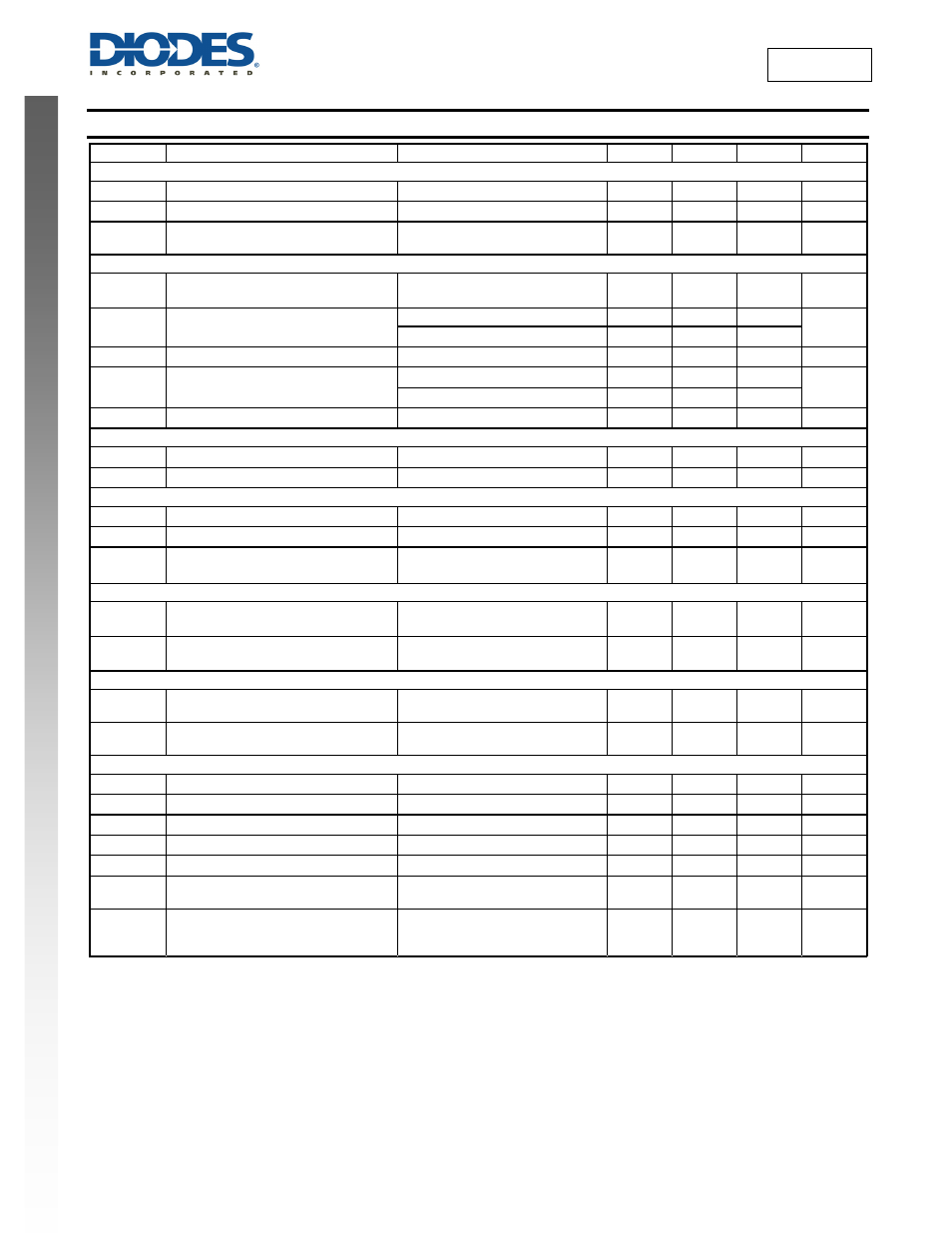
Electrical Characteristics
(V
DD
= 12V, C
L
= 100µF, dv/dt pin open, R
LIMIT
= 10
Ω, and T
A
= +25°C, unless otherwise noted.)
Symbol
Characteristic
Test Condition
Min
Typ
Max
Unit
Device
I
BIAS
Bias current
Device operational
—
0.8
1.5
mA
I
BIAS_SD
Bias current during shutdown
Device shutdown
—
0.4
mA
V
DD_MIN
Minimum operating voltage once
successfully started up
—
—
7.6
V
NMOS Power Device
T
DLY
Chip enable dealy time
Enabling of the IC to I
D
= 100mA
(with 1A resistive load)
— 220 — us
R
DSON
NMOS Drain to source Kelvin ON
Resistance (Note 7)
NMOS fully on
20
30
40
m
Ω
NMOS fully on, T
J
= +140
°C
—
45 —
V
OUT_OFF
Off state output voltage
V
DD
= 18V, V
GS
= 0V, R
L
= ∞
—
0.19 0.3 V
I
D
Continuous current (Note 8)
T
A
= +25
°C, 0.5 in.
2
pad
—
3.6
—
A
T
A
= +80
°C, min copper
—
1.7
—
Output
capacitance
V
DS
= 12V, V
GS
= 0V, f = 1MHz
—
250
—
pF
dv/dt Ramp
T
SLEW
Output voltage ramp time
Device enable to V
DS
= 11.7V
1.5 1.8 2.5 ms
V
C_MAX
Maximum capacitor voltage
— —
V
DD
V
Under/Over Voltage Protection
V
UVLO
Under voltage lockout threshold
Turn on, Voltage rising
7.7
8.5
9.3
V
V
UVLO_HYST
Under voltage lockout hysteresis
—
0.80
—
V
V
CLAMP
Over voltage clamp limit (Note 9)
During over voltage protection,
V
DD
= 18V
14 15
16.2 V
Current Limit
I
LIMIT_SS
Kelvin short circuit current limit
(Note 10)
R
LIMIT
= 15.4
Ω
2.75 3.44 4.25 A
I
LIMIT_OL
Kelvin over load current limit
(Note 10)
R
LIMIT
= 15.4
Ω
— 4.6 — A
Thermal Protection
T
SD
Thermal shutdown junction temperature
threshold (Note 8)
Temperature rising
150
175
200
°C
T
SD_HYST
Thermal shutdown hysteresis in non
latching devices
—
45
—
°C
Enable/Fault
V
EN_LOW
Enble logic level low voltage
Output disabled
0.35
0.58
0.81
V
V
EN_MID
Enble logic level mid voltage
Output disabled, Thermal fault
0.82
1.4
1.95
V
V
EN_HI
Enble logic level high
Output enabled
1.96
2.64
3.3
V
V
EN_MAX
High state maximum voltage
3.4
4.3
5.3
V
I
EN_SINK
Logic low sink current
V
ENABLE
= 0V
— -17 -25 uA
I
EN_LKG
Logic high leakage current for external
switch
V
ENABLE
= 3.3V
— — 1.0
uA
Fanout
Maximum fanout – number of device that
can be connected together to this pin for
simultaneous shutdown
—
—
3.0
Units
Notes:
7. Pulse test with pulse width of 300µs, dyty cycle 2%.
8. This parameter is not tested in production. It is guaranteed by design, process control and characterization.
9. Over voltage clamp feature is available on in NIS5132MN1 and NIS5132MN2 versions.
10. Refer to application note on explanation on short circuit and overload conditions.