New prod uc t nis5132 absolute maximum ratings, Recommended operating conditions – Diodes NIS5132 User Manual
Page 4
NIS5132
Document number: DS36457 Rev. 1 - 5
4 of 11
December 2013
© Diodes Incorporated
NEW PROD
UC
T
NIS5132
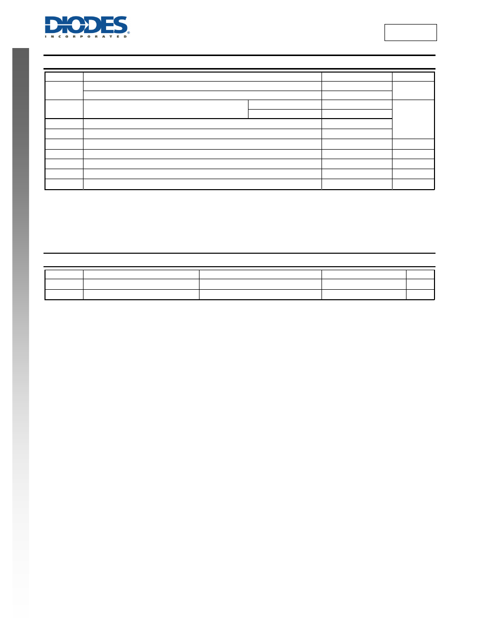
Absolute Maximum Ratings
(Note 4) (@T
A
= +25°C, unless otherwise specified.)
Symbol Characteristic
Value
Unit
V
DD
Input voltage in steady state operating conditions (Note 5)
-0.6 to +18
V
Input voltage - transient (100ms)
-0.6 to +25
θ
JA
Junction to air thermal resistance
0.1 in
2
(Note 6)
227
°C/W
0.5 in
2
(Note 6)
95
θ
JL
Junction to lead thermal resistance
27
θ
JC
Junction to case thermal resistance
20
P
DMAX
Package Power Dissipation at T
A
= +25
°C
1.3 W
Thermal derating above +25
°C
10.4 (TBD)
mW/
°C
Ts
Storage temperature range
-55 to +155
°C
T
J
Operating junction temperature (Note 7)
-40 to +150
°C
T
L
Lead temperature during soldering (10s)
260
°C
Notes:
4. Stresses greater than the 'Absolute Maximum Ratings' specified above may cause permanent damage to the device. These are stress ratings
only; functional operation of the device at these or any other conditions exceeding those indicated in this specification is not implied. Device
reliability may be affected by exposure to absolute maximum rating conditions for extended periods of time.
5. Negative voltage will not damage the device provided that the power dissipation is within the package package dissipation rating.
6. 1 oz copper on double sided FR4 PCB
7. Thermal limit is set above the maximum thermal rating. It is not recommended to operate the device at temperature above the maximum rating
for extended period.
Recommended Operating Conditions
Symbol Characteristic
Test
Condition
Rating
Unit
V
DD
Supply Voltage
Operating
9.0 to 18.0
V
T
J
Operating Juntion Temperature Range
Operating
-40 to +150
°C