New prod uc t nis5132 typical application circuits, Pin descriptions – Diodes NIS5132 User Manual
Page 2
NIS5132
Document number: DS36457 Rev. 1 - 5
2 of 11
December 2013
© Diodes Incorporated
NEW PROD
UC
T
NIS5132
Typical Application Circuits
(cont.)
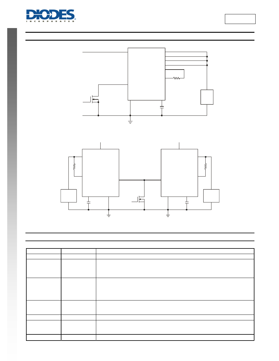
Figure 2 Application Circuit with Kelvin Current Sensing
Figure 3 Application Circuit with Common Thermal Shutdown
Pin Descriptions
Package: U-DFN3030-10
Pin Number
Pin Name
Function
1
GND
Ground pin
2 dv/dt
Internal NMOS power device turn-on time adjustment pin:
If this pin is is left unconnected, the internal capacitor ensures the turn-on ramp is over a
period of 2ms typical. If an additional delay is required, connect a capacitor from this pin to the
ground.
3 Enable/Fault
Tri-state bi-directional interface pin:
The output can be disabled by pulling this pin to ground through an open drain or an open
collector. Additionally, this pin output goes to an intermediate state to indicate that the device
is in thermal shutdown state. This pin can also be connected together with other NIS5132
devices to cause a system-wide simultaneous shutdown during thermal events.
4
I
LIMIT
Current limit setting pin:
A resistor between Source pins and this pin sets the overload and short-circuit current limit
thresholds.
5 NC
No
connect
6 to 10
Source
The internal NMOS power device’s Source pins:
These pins are the Source of internal power device and also the output terminal of the
electronic fuse
Exposed PAD
V
DD
Positive input voltage to the device
V
DD
SOURCE
I
LIMIT
ENABLE
GND
dv/dt
LOAD
ENABLE
NIS5132
LOAD
V
DD
SOURCE
I
LIMIT
ENABLE
GND
dv/dt
NIS5132
R
S
+12V
ENABLE
GND
GND
dv/dt
LOAD
ENABLE
V
DD
SOURCE
I
LIMIT
10
9
8
7
6
4
3
11
1
2
NIS5132
R
S