Maximum ratings, total device, Thermal characteristics, Maximum ratings: pre-biased pnp transistor (q1) – Diodes LMN400E01 User Manual
Page 2
LMN400E01
Document number: DS30750 Rev. 8 - 2
2 of 10
July 2011
© Diodes Incorporated
LMN400E01
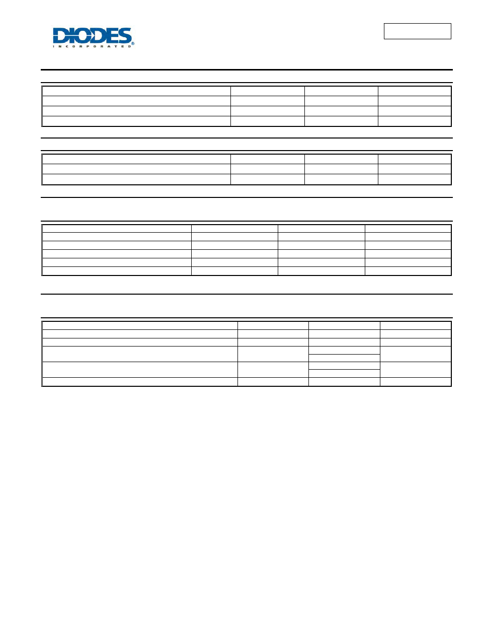
Maximum Ratings, Total Device
@T
A
= 25°C unless otherwise specified
Characteristic
Symbol
Value
Unit
Power Dissipation (Note 4)
P
D
200
mW
Power Derating Factor above 37.5
°C
P
der
1.6
mW/°C
Output Current
I
out
400 mA
Thermal Characteristics
@T
A
= 25°C unless otherwise specified
Characteristic
Symbol
Value
Unit
Operating and Storage Temperature Range
T
j
, T
STG
-55 to +150
°C
Thermal Resistance, Junction to Ambient Air (Note 4)
R
θJA
625
°C/W
Maximum Ratings:
Pre-Biased PNP Transistor (Q1)
@T
A
= 25°C unless otherwise specified
Characteristic
Symbol
Value
Unit
Collector-Base Voltage
V
CBO
-50
V
Collector-Emitter Voltage
V
CEO
-50
V
Supply Voltage
V
cc
-50
V
Input Voltage
V
in
-6 to +5
V
Output Current
I
C
-400 mA
Maximum Ratings:
ESD Protected N-Channel MOSFET (Q2)
@T
A
= 25°C unless otherwise specified
Characteristic
Symbol
Value
Unit
Drain-Source Voltage
V
DSS
60
V
Drain Gate Voltage (R
GS
≤ 1M Ohm)
V
DGR
60
V
Gate-Source Voltage Continuous
Pulsed (tp<50 uS)
V
GSS
+/-20
V
+/-40
Drain Current (Note 4) Continuous (V
gs
= 10V)
Pulsed (tp <10 uS, Duty Cycle <1%)
I
D
300
mA
800
Continuous Source Current
I
S
300 mA
Notes:
4. Device mounted on FR-4 PCB, 1 inch x 0.85 inch x 0.062 inch; pad layout as shown on Diodes Inc. suggested pad layout document AP02001,
which can be found on our website at