Diodes LMN200B02 User Manual
General description, Features, Mechanical data
DS30658 Rev. 7 - 2
1 of 9
www.diodes.com
LMN200B02
© Diodes Incorporated
LMN200B02
200 mA LOAD SWITCH FEATURING PRE-BIASED PNP TRANSISTOR AND N-MOSFET
WITH GATE PULL DOWN RESISTOR
General Description
LMN200B02 is best suited for applications where the load needs to
be turned on and off using control circuits like micro-controllers,
comparators etc. particularly at a point of load. It features a
discrete pass transistor with stable V
CE(SAT)
which does not
depend on the input voltage and can support continuous maximum
current of 200 mA . It also contains a discrete N-MOSFET that can
be used as control. This N-MOSFET also has a built-in pull down
resistor at its gate. The component can be used as a part of a
circuit or as a stand alone discrete device.
Features
•
Voltage Controlled Small Signal Switch
•
N-MOSFET with Gate Pull-Down Resistor
•
Surface Mount Package
•
Ideally Suited for Automated Assembly Processes
•
Lead Free By Design/RoHS Compliant (Note 1)
•
"Green" Device (Note 2)
Mechanical Data
• Case:
SOT-363
•
Case Material: Molded Plastic, “Green” Molding Compound.
UL Flammability Classification Rating 94V-0
•
Moisture Sensitivity: Level 1 per J-STD-020
•
Terminal Connections: See Diagram
•
Terminals: Finish - Matte Tin annealed over Alloy 42
leadframe. Solderable per MIL-STD-202, Method 208
•
Marking Information: See Page 8
•
Ordering Information: See Page 8
•
Weight: 0.006 grams (approximate)
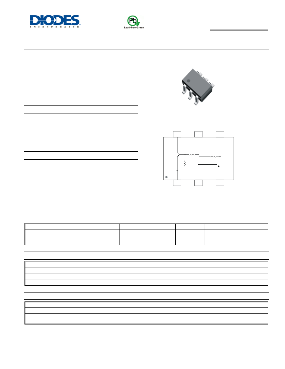
Sub-Component P/N
Reference
Device Type
R1 (NOM)
R2 (NOM)
R3 (NOM)
Figure
DDTB142JU_DIE Q1
PNP
Transistor
10K
470
⎯
2
DSNM6047_DIE (with Gate Pull-Down
Resistor)
Q2 N-MOSFET
⎯
⎯
37K 2
Maximum Ratings, Total Device
@T
A
= 25°C unless otherwise specified
Characteristic
Symbol
Value
Unit
Power Dissipation (Note 3)
P
D
200
mW
Power Derating Factor above 125°C
P
der
1.6
mW/°C
Output Current
I
out
200
mA
Thermal Characteristics
@T
A
= 25°C unless otherwise specified
Characteristic
Symbol
Value
Unit
Operating and Storage Temperature Range
T
J
,T
STG
-55 to +150
°C
Thermal Resistance, Junction to Ambient Air (Equivalent to
One Heated Junction of PNP Transistor) (Note 3)
R
θJA
625
°C/W
Notes:
1. No purposefully added lead.
2. Diodes Inc.'s "Green" policy can be found on our website
3. Device mounted on FR-4 PCB, 1 inch x 0.85 inch x 0.062 inch; pad layout as shown on Diodes Inc. suggested pad layout document AP02001,
which can be found on our website
Fig. 1: SOT-363
S
D
G
C
E
B
Q2
NMOS
R3
37K
R2
470
Q1
PNP
R1
10K
1
2
3
4
5
6
C_Q1
E_Q1
G_Q2
D_Q2
S_Q2
B_Q1
DSNM6047_DIE
DDTB142JU_DIE
Fig. 2 Schematic and Pin Configuration
1
2
3
4
5
6