Diodes DMP2540UCB9 User Manual
Product summary, Description and applications, Features and benefits
DMP2540UCB9
Document number: DS35611 Rev. 4 - 2
1 of 6
June 2012
© Diodes Incorporated
DMP2540UCB9
NEW PROD
UC
T
ADVAN
CE I
N
F
O
RM
ATI
O
N
P-CHANNEL ENHANCEMENT MODE MOSFET
Product Summary
V
(BR)DSS
R
DS(ON)
I
D
T
A
= 25°C
-25V
40m
Ω @ V
GS
= -4.5V
-5.2 A
Description and Applications
This new generation MOSFET has been designed to minimize the on-
state resistance (R
DS(on)
) and yet maintain superior switching
performance, making it ideal for high efficiency power management
applications.
•
Battery Management
• Load
Switch
• Battery
Protection
Features and Benefits
• Low
Q
g
& Q
gd
•
Small Footprint 1.5-mm × 1.5-mm
•
Gate ESD Protection 6kV
•
Totally Lead-Free & Fully RoHS Compliant (Notes 1 & 2)
•
Halogen and Antimony Free. “Green” Device (Note 3)
•
Qualified to AEC-Q101 Standards for High Reliability
Mechanical Data
• Case:
U-WLB1515-9
•
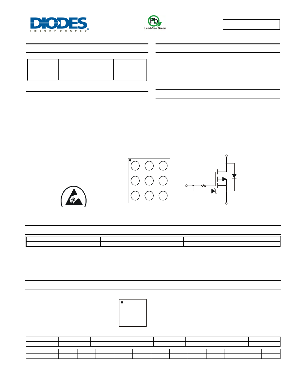
Terminal Connections: See Diagram Below
•
Weight: 0.0018 grams (approximate)
Ordering Information
(Note 4)
Part Number
Case
Packaging
DMP2540UCB9-7
U-WLB1515-9
3000/Tape & Reel
Notes:
1. No purposely added lead. Fully EU Directive 2002/95/EC (RoHS) & 2011/65/EU (RoHS 2) compliant.
2. Se information about Diodes Incorporated’s definitions of Halogen- and Antimony-free, "Green" and Lead-free.
3. Halogen- and Antimony-free "Green” products are defined as those which contain <900ppm bromine, <900ppm chlorine (<1500ppm total Br + Cl) and
<1000ppm antimony compounds.
4. For packaging details, go to our website at
Marking Information
Date Code Key
Year
2011
2012
2013
2014
2015
2016
2017
Code Y
Z
A
B
C D
E
Month
Jan
Feb
Mar
Apr
May
Jun
Jul
Aug
Sep
Oct
Nov
Dec
Code 1 2 3 4 5 6 7 8 9 O N D
Top-View
Pin Configuration
3W
YM
3W = Product Type Marking Code
YM = Date Code Marking
Y = Year (ex: Y = 2011)
M = Month (ex: 9 = September)
G
D
S
D
D
S
D
S
S
Equivalent Circuit
ESD PROTECTED TO 6kV
Source
Gate
Protection
Diode
Gate
Drain