Dmp1055ufdb, Package outline dimensions, Suggested pad layout – Diodes DMP1055UFDB User Manual
Page 5
DMP1055UFDB
Document number: DS36934 Rev.1 - 2
5 of 6
April 2014
© Diodes Incorporated
DMP1055UFDB
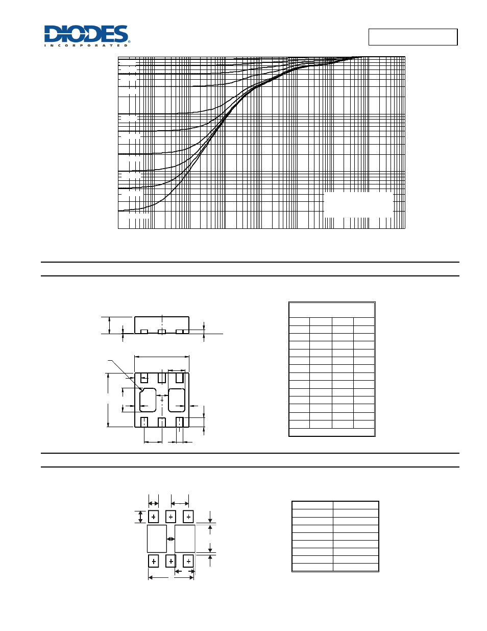
Package Outline Dimensions
rsion.
Suggested Pad Layout
e latest version.
t1, PULSE DURATION TIMES (sec)
Figure 12 Transient Thermal Resistance
r(t
),
T
R
ANS
IEN
T
T
H
E
R
MA
L
R
ES
IS
TAN
C
E
R
(t) = r(t) * R
R
= 159°C/W
Duty Cycle, D = t1/ t2
JA
JA
JA
D = 0.7
D = 0.5
D = 0.3
D = 0.1
D = 0.05
D = 0.02
D = 0.01
D = 0.005
Single Pulse
0.001
0.01
0.1
1
0.00001
0.0001
0.001
0.01
0.1
1
10
100
1000
D = 0.9
U-DFN2020-6
Type B
Dim
Min
Max Typ
A
0.545 0.605 0.575
A1
0 0.05
0.02
A3
0.13
b
0.20
0.30 0.25
D
1.95 2.075 2.00
d
0.45
D2
0.50 0.70 0.60
e
0.65
E
1.95 2.075 2.00
E2
0.90 1.10 1.00
f
0.15
L
0.25 0.35 0.30
z
0.225
All Dimensions in mm
Dimensions Value (in mm)
Z
1.67
G
0.20
G1 0.40
X1 1.0
X2
0.45
Y 0.37
Y1 0.70
C 0.65
SEATING PLANE
D
e
Pin#1 ID
L
b
D2
E2
E
A1
A
A3
f
z
f
d
G
G
Y
C
Z
Y1
X2
X1
G1
- PDS3200 (5 pages)
- PDS340 (5 pages)
- PDS340Q (5 pages)
- PDS360 (5 pages)
- PDS360Q (5 pages)
- PDS4150 (4 pages)
- PDS3100Q (5 pages)
- PDS3100 (5 pages)
- PDS1240CTL (5 pages)
- PDS1045 (5 pages)
- PDS1040L (5 pages)
- PDS1040CTL (5 pages)
- PDS1040 (5 pages)
- PD3S230L (5 pages)
- PD3S230H (3 pages)
- PDS5100Q (5 pages)
- PDS835L (5 pages)
- PDS760 (5 pages)
- PDS560 (5 pages)
- PDS540 (5 pages)
- PDS5100H (5 pages)
- PDS5100 (5 pages)
- PDS4200H (6 pages)
- SBL3060CTP (4 pages)
- SBL30L30CT (3 pages)
- SBL3045CTP (4 pages)
- SBL3040CTP (4 pages)
- SBL2060CTP (4 pages)
- SBL2030CT - SBL2060CT (3 pages)
- SBL2045CTP (4 pages)
- SBL1060CTP (4 pages)
- SBL1040CTP (4 pages)
- SBG3030CT - SBG3045CT (5 pages)
- SB520 - SB560 (3 pages)
- SB370 - SB3100 (3 pages)
- SB320 - SB360 (3 pages)
- SBR10U100CT (5 pages)
- SBR10U150CT (5 pages)
- SBR10A45SP5 (5 pages)
- SBR1060CT (5 pages)
- SBR1045SP5 (5 pages)
- SBR1045SD1 (4 pages)
- SBR1045D1 (5 pages)
- SBR1045CTL (4 pages)
- SBR1040CT (5 pages)