Electrical characteristics, Dms3016sfg – Diodes DMS3016SFG User Manual
Page 3
POWERDI is a registered trademark of Diodes Incorporated.
DMS3016SFG
Document number: DS35434 Rev. 7 - 2
3 of 7
October 2012
© Diodes Incorporated
DMS3016SFG
0.001
0.01
0.1
1
0.00001
0.0001
0.001
0.01
0.1
1
10
100
1,000
t1, PULSE DURATION TIMES (sec)
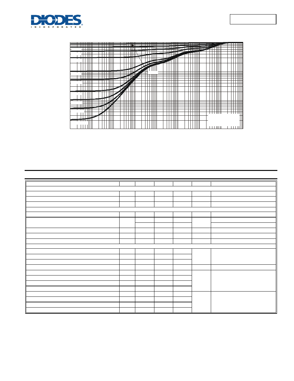
Fig. 3 Transient Thermal Resistance
R
(t)=r(t) * R
θJA
R
= 54°C/W
Duty Cycle, D = t1/ t2
θ
θ
JA
JA
r(
t)
, T
R
ANSI
ENT T
H
ERM
A
L
RE
SI
ST
ANCE
D = 0.9
D = 0.7
D = 0.5
D = 0.3
D = 0.1
D = 0.05
D = 0.02
D = 0.01
D = 0.005
Single Pulse
Electrical Characteristics
(@T
A
= +25°C, unless otherwise specified.)
Characteristic Symbol
Min
Typ
Max
Unit
Test
Condition
OFF CHARACTERISTICS (Note 8)
Drain-Source Breakdown Voltage
BV
DSS
30
⎯
⎯
V
V
GS
= 0V, I
D
= 1mA
Zero Gate Voltage Drain Current
I
DSS
⎯
⎯
100
µA
V
DS
= 30V, V
GS
= 0V
Gate-Source Leakage
I
GSS
⎯
⎯
±100
nA
V
GS
=
±12V, V
DS
= 0V
ON CHARACTERISTICS (Note 8)
Gate Threshold Voltage
V
GS(th)
1.0
⎯
2.2 V
V
DS
= V
GS
, I
D
= 250
μA
Static Drain-Source On-Resistance
R
DS(ON)
⎯
10 13
m
Ω
V
GS
= 10V, I
D
= 11.2A
⎯
12 16
V
GS
= 4.5V, I
D
= 10.A
Forward Transfer Admittance
|Y
fs
|
⎯
25
⎯
S
V
DS
= 5V, I
D
= 11.2A
Diode Forward Voltage
V
SD
⎯
0.37 0.6 V
V
GS
= 0V, I
S
= 1A
Maximum Body-Diode + Schottky Continuous Current
I
S
⎯
⎯
5 A
DYNAMIC CHARACTERISTICS (Note 9)
Input Capacitance
C
iss
⎯
1886
⎯
pF
V
DS
= 15V, V
GS
= 0V
f = 1.0MHz
Output Capacitance
C
oss
⎯
372
⎯
Reverse Transfer Capacitance
C
rss
⎯
128
⎯
Gate Resistance
R
G
⎯
2.0
⎯
Ω
V
DS
= 0V, V
GS
= 0V, f = 1.0MHz
Total Gate Charge (V
GS
= 4.5V)
Q
g
⎯
19.5
⎯
nC
V
DS
= 15V, V
GS
= 10V
I
D
= 11.2A
Total Gate Charge (V
GS
= 10V)
Q
g
⎯
44.6
⎯
Gate-Source Charge
Q
gs
⎯
4.8
⎯
Gate-Drain Charge
Q
gd
⎯
4.6
⎯
Turn-On Delay Time
t
D(on)
⎯
5.8
⎯
ns
V
GS
= 10V, V
DD
= 15V, R
G
= 3
Ω,
R
L
= 1.2
Ω
Turn-On Rise Time
t
r
⎯
23.7
⎯
Turn-Off Delay Time
t
D(off)
⎯
35.4
⎯
Turn-Off Fall Time
t
f
⎯
7.7
⎯
Notes:
8 .Short duration pulse test used to minimize self-heating effect.
9. Guaranteed by design. Not subject to production testing.