Marking information, Maximum ratings, Thermal characteristics – Diodes DMS3016SFG User Manual
Page 2: Dms3016sfg, S30 yyw w
POWERDI is a registered trademark of Diodes Incorporated.
DMS3016SFG
Document number: DS35434 Rev. 7 - 2
2 of 7
October 2012
© Diodes Incorporated
DMS3016SFG
Marking Information
Maximum Ratings
(@T
A
= +25°C, unless otherwise specified.)
Characteristic Symbol
Value
Units
Drain-Source Voltage
V
DSS
30 V
Gate-Source Voltage
V
GSS
±12 V
Continuous Drain Current (Note 5) V
GS
= 10V
Steady
State
T
A
= +25°C
T
A
= +70°C
I
D
7.0
5.5
A
Continuous Drain Current (Note 5) V
GS
= 4.5V
Steady
State
T
A
= +25°C
T
A
= +70°C
I
D
6.4
5.1
A
Continuous Drain Current (Note 6) V
GS
= 10V
Steady
State
T
A
= +25°C
T
A
= +70°C
I
D
10.2
8.1
A
Continuous Drain Current (Note 6) V
GS
= 4.5V
Steady
State
T
A
= +25°C
T
A
= +70°C
I
D
9.3
7.4
A
Pulsed Drain Current (10us pulse, duty cycle=1%)
I
DM
80 A
Avalanche Current (Note 7)
I
AR
13 A
Repetitive Avalanche Energy (Note 7) L = 0.3mH
E
AR
24 mJ
Thermal Characteristics
(@T
A
= +25°C, unless otherwise specified.)
Characteristic Symbol
Value
Units
Total Power Dissipation
(Note 5)
P
D
0.98
2.08
W
(Note 6)
Thermal Resistance, Junction to Ambient
(Note 5)
R
θJA
127
60
°C/W
(Note 6)
Thermal Resistance, Junction to Case
(Note 6)
R
θJC
3.42 °C/W
Operating and Storage Temperature Range
T
J,
T
STG
-55 to +150
°C
Notes:
5. Device mounted on FR-4 PC board, with minimum recommended pad layout, single sided.
6. Device mounted on FR-4 substrate PC board, 2oz copper, with thermal vias to bottom layer 1inch square copper plate
7 .I
AR
and E
AR
rating are based on low frequency and duty cycles to keep T
J
= +25°C
V
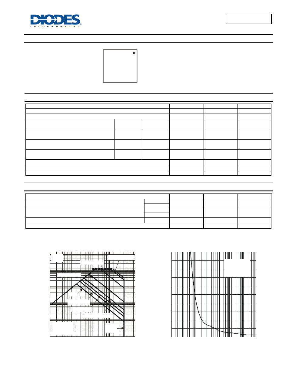
, DRAIN-SOURCE VOLTAGE (V)
DS
Fig. 1 SOA, Safe Operation Area
I
, DRA
IN CURREN
T
(
A
)
D
0.01
0.1
1
10
100
1,000
0.01
0.1
1
10
100
I (A) @P =10s
D
W
I (A) @ DC
D
I (A) @P =1s
D
W
I (A) @P =100ms
D
W
I (A) @P =10ms
D
W
T
= 150 C
T = 25 C
Single Pulse
J(MAX)
A
°
°
I (A) @P =1ms
D
W
I (A) @
P =10µs
D
W
I (A) @P =100µs
D
W
R
Limited
DS(ON)
t1, PULSE DURATION TIME (sec)
Fig. 2 Single Pulse Maximum Power Dissipation
0.001 0.01
0.1
1
10
100
1,000
0.0001
0
10
20
30
40
50
60
70
80
90
100
P
,
P
EAK
T
R
A
N
SI
E
N
T
P
O
IW
E
R
(W
)
(P
K
)
Single Pulse
R
= 54 C/W
R
= r
* R
T - T = P * R
θ
θ
θ
θ
JA
JA(t)
(t)
JA
J
A
JA(t)
°
S30
YYW
W
S30 = Product Type Marking Code
YYWW = Date Code Marking
YY = Last digit of year (ex: 09 = 2009)
WW = Week code (01 ~ 53)