Package outline dimensions, Suggested pad layout – Diodes DMN3026LVT User Manual
Page 5
DMN3026LVT
Document number: DS36813 Rev. 3 - 2
5 of 6
April 2014
© Diodes Incorporated
DMN3026LVT
ADVAN
CE I
N
F
O
RM
ATI
O
N
ADVANCED INFORMATION
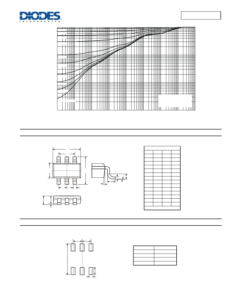
Package Outline Dimensions
rsion.
Suggested Pad Layout
rsion.
t1, PULSE DURATION TIME (sec)
Figure 13 Transient Thermal Resistance
r(t
),
T
R
A
N
SI
EN
T
T
H
E
R
MA
L
R
ES
IS
TAN
C
E
R
(t) = r(t) * R
R
= 97°C/W
Duty Cycle, D = t1/ t2
JA
JA
JA
D = 0.5
D = 0.7
D = 0.9
D = 0.3
D = 0.1
D = 0.05
D = 0.02
D = 0.01
D = 0.005
D = Single Pulse
0.001
0.01
0.1
1
0.00001
0.0001
0.001
0.01
0.1
1
10
100
1000
TSOT26
Dim
Min Max Typ
A
— 1.00 —
A1 0.01 0.10 —
A2 0.84 0.90 —
D
— — 2.90
E
— — 2.80
E1
— — 1.60
b
0.30 0.45 —
c
0.12 0.20 —
e
— — 0.95
e1
— — 1.90
L
0.30 0.50 —
L2
— — 0.25
θ
0° 8° 4°
θ1
4° 12° —
All Dimensions in mm
Dimensions Value (in mm)
C
0.950
X
0.700
Y
1.000
Y1
3.199
c
A1
L
E1
E
A2
D
e1
e
6x b
4x 1
L2
A
Y1
C
C
X (6x)
Y (6x)
- PDS3200 (5 pages)
- PDS340 (5 pages)
- PDS340Q (5 pages)
- PDS360 (5 pages)
- PDS360Q (5 pages)
- PDS4150 (4 pages)
- PDS3100Q (5 pages)
- PDS3100 (5 pages)
- PDS1240CTL (5 pages)
- PDS1045 (5 pages)
- PDS1040L (5 pages)
- PDS1040CTL (5 pages)
- PDS1040 (5 pages)
- PD3S230L (5 pages)
- PD3S230H (3 pages)
- PDS5100Q (5 pages)
- PDS835L (5 pages)
- PDS760 (5 pages)
- PDS560 (5 pages)
- PDS540 (5 pages)
- PDS5100H (5 pages)
- PDS5100 (5 pages)
- PDS4200H (6 pages)
- SBL3060CTP (4 pages)
- SBL30L30CT (3 pages)
- SBL3045CTP (4 pages)
- SBL3040CTP (4 pages)
- SBL2060CTP (4 pages)
- SBL2030CT - SBL2060CT (3 pages)
- SBL2045CTP (4 pages)
- SBL1060CTP (4 pages)
- SBL1040CTP (4 pages)
- SBG3030CT - SBG3045CT (5 pages)
- SB520 - SB560 (3 pages)
- SB370 - SB3100 (3 pages)
- SB320 - SB360 (3 pages)
- SBR10U100CT (5 pages)
- SBR10U150CT (5 pages)
- SBR10A45SP5 (5 pages)
- SBR1060CT (5 pages)
- SBR1045SP5 (5 pages)
- SBR1045SD1 (4 pages)
- SBR1045D1 (5 pages)
- SBR1045CTL (4 pages)
- SBR1040CT (5 pages)