Electrical characteristics, Dmn1019ufde – Diodes DMN1019UFDE User Manual
Page 3
DMN1019UFDE
D
atasheet number: DS35561 Rev. 5 - 2
3 of 7
October 2013
© Diodes Incorporated
DMN1019UFDE
ADVAN
CE I
N
F
O
RM
ATI
O
N
Electrical Characteristics
(@T
A
= +25°C, unless otherwise specified.)
Characteristic
Symbol
Min
Typ
Max
Unit
Test Condition
OFF CHARACTERISTICS (Note 7)
Drain-Source Breakdown Voltage
BV
DSS
12
— — V
V
GS
= 0V, I
D
= 250μA
Zero Gate Voltage Drain Current T
J
= +25°C
I
DSS
—
—
1 µA
V
DS
= 12V, V
GS
= 0V
Gate-Source Leakage
I
GSS
—
—
±2 µA
V
GS
= ±8V, V
DS
= 0V
ON CHARACTERISTICS (Note 7)
Gate Threshold Voltage
V
GS(th)
0.35 — 0.8 V
V
DS
= V
GS
, I
D
= 250μA
Static Drain-Source On-Resistance
R
DS (ON)
—
7 10
mΩ
V
GS
= 4.5V, I
D
= 9.7A
8 12
V
GS
= 2.5V, I
D
= 9A
10 14
V
GS
= 1.8V, I
D
= 8.1A
14 18
V
GS
= 1.5V, I
D
= 4.5A
28 41
V
GS
= 1.2V, I
D
= 2.4A
Forward Transfer Admittance
|Y
fs
|
—
28 — S
V
DS
= 4V, I
D
= 9.7A
Diode Forward Voltage
V
SD
—
0.8 1.2 V V
GS
= 0V, I
S
= 10A
DYNAMIC CHARACTERISTICS (Note 8)
Input Capacitance
C
iss
— 2425 —
pF
V
DS
= 10V, V
GS
= 0V,
f = 1.0MHz
Output Capacitance
C
oss
— 396 —
Reverse Transfer Capacitance
C
rss
— 375 —
Gate Resistance
R
g
— 1.1 — Ω
V
DS
= 0V, V
GS
= 0V, f = 1MHz
Total Gate Charge (V
GS
= 8V)
Q
g
— 50.6 —
nC
V
DS
= 4V, I
D
= 10A
Total Gate Charge (V
GS
= 4.5V)
Q
g
— 27.3 —
Gate-Source Charge
Q
gs
— 3.4 —
Gate-Drain Charge
Q
gd
— 5.2 —
Turn-On Delay Time
t
D(on)
— 7.6 —
ns
V
DD
= 4V, V
GS
= 10V, I
D
= 10A
R
G
= 1Ω, R
L
= 0.4Ω
Turn-On Rise Time
t
r
— 22.2 —
Turn-Off Delay Time
t
D(off)
— 57.6 —
Turn-Off Fall Time
t
f
— 16.8 —
Notes:
5. Device mounted on FR-4 PC board, with minimum recommended pad layout, single sided.
6. Device mounted on FR-4 substrate PC board, 2oz copper, with thermal bias to bottom layer 1inch square copper plate.
7. Short duration pulse test used to minimize self-heating effect.
8. Guaranteed by design. Not subject to production testing.
0.00001
0.0001
0.001
0.01
0.1
1
10
100
1,000
t1, PULSE DURATION TIME (sec)
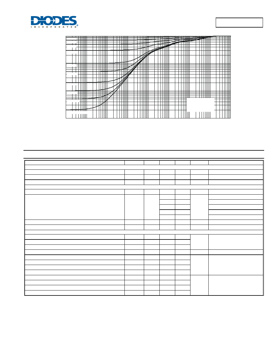
Fig. 3 Transient Thermal Resistance
0.001
0.01
0.1
1
r(t
),
T
R
AN
SI
EN
T
T
H
E
R
MA
L
R
ES
IS
TAN
C
E
R
= r * R
JA(t)
(t)
JA
JA
R
= 178 C/W
Duty Cycle, D = t1/t2
D = 0.5
D = 0.7
D = 0.9
D = 0.3
D = 0.1
D = 0.05
D = 0.02
D = 0.01
D = 0.005
D = Single Pulse