Maximum ratings, Thermal characteristics, Dmn1019ufde – Diodes DMN1019UFDE User Manual
Page 2
DMN1019UFDE
D
atasheet number: DS35561 Rev. 5 - 2
2 of 7
October 2013
© Diodes Incorporated
DMN1019UFDE
ADVAN
CE I
N
F
O
RM
ATI
O
N
Maximum Ratings
(@T
A
= +25°C, unless otherwise specified.)
Characteristic Symbol
Value
Units
Drain-Source Voltage
V
DSS
12 V
Gate-Source Voltage
V
GSS
±8 V
Continuous Drain Current (Note 5) V
GS
= 4.5V
Steady
State
T
A
= +25°C
T
A
= +70°C
I
D
11
9
A
t<5s
T
A
= +25°C
T
A
= +70°C
I
D
14
11
A
Maximum Continuous Body Diode Current
I
S
3.0 A
Pulsed Drain Current (10µs pulse, duty cycle = 1%)
I
DM
100 A
Thermal Characteristics
Characteristic Symbol
Value
Units
Total Power Dissipation (Note 5)
T
A
= +25°C
P
D
0.69
0.44
W
T
A
= +70°C
Thermal Resistance, Junction to Ambient (Note 5)
Steady state
R
JA
182
118
°C/W
t<5s
Total Power Dissipation (Note 6)
T
A
= +25°C
P
D
2.17
1.38
W
T
A
= +70°C
Thermal Resistance, Junction to Ambient (Note 6)
Steady state
R
JA
58
38
°C/W
t<5s
Thermal Resistance, Junction to Case (Note 6)
R
Jc
10
Operating and Storage Temperature Range
T
J,
T
STG
-55 to +150
°C
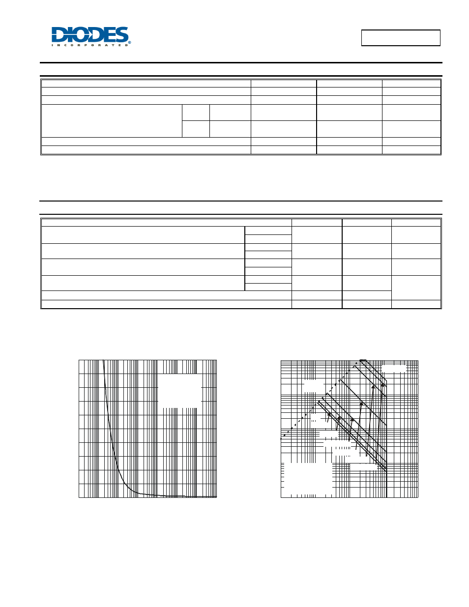
t1, PULSE DURATION TIME (sec)
Fig. 1 Single Pulse Maximum Power Dissipation
0.001 0.01
0.1
1
10
100 1,000
0.0001
0
10
20
30
40
50
60
70
80
90
100
P
, P
E
AK
T
R
ANS
IEN
T
P
O
IW
E
R
(W
)
(P
K
)
Single Pulse
R
= 178 C/W
R
= r * R
T - T = P * R
JA
JA(t)
(t)
JA
J
A
JA(t)
DUT on MRP
0.01
0.1
1
10
100
V , DRAIN-SOURCE VOLTAGE (V)
Fig. 2 SOA, Safe Operation Area
DS
0.01
0.1
1
10
100
I,
D
R
AI
N
C
U
R
R
EN
T
(A
)
D
R
Limited
DS(on)
DC
P = 10s
W
P = 1s
W
P = 100ms
W
P = 10ms
W
P = 1ms
W
P = 100µs
W
P = 10 s
W
µ
T
= 150°C
T = 25°C
Single Pulse
DUT on 1 * MRP Board
V
= 8V
J(max)
A
GS