Thermal characteristics and derating information, Safe operating area, Derating curve – Diodes DSS60601MZ4 User Manual
Page 3: Transient thermal impedance, Pulse power dissipation
DSS60601MZ4
Document number: DS31587 Rev. 3 - 2
3 of 8
www.diodes.com
March 2014
© Diodes Incorporated
DSS60601MZ4
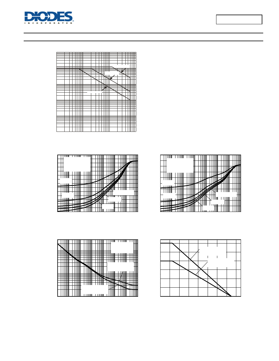
Thermal Characteristics and Derating Information
100µ
1m
10m 100m
1
10
100
1k
0
10
20
30
40
50
60
70
1
10
10m
100m
1
10
1
10
10m
100m
1
10
T
amb
=25°C
25mm x 25mm
2oz FR4
V
CE(sat)
Limit
100µs
1ms
10ms
100ms
1s
DC
Safe Operating Area
I
C
Co
lle
ct
or Curre
nt
(A
)
V
CE
Collector-Emitter Voltage (V)
0
20
40
60
80 100 120 140 160
0.0
0.5
1.0
1.5
2.0
2.5
3.0
50mm x 50mm
2oz FR4
25mm x 25mm
2oz FR4
Derating Curve
Temperature (°C)
M
a
x P
ow
er
D
is
si
p
at
ion (
W
)
100µ
1m
10m 100m
1
10
100
1k
0
10
20
30
40
50
T
amb
=25°C
25mm x 25mm
2oz FR4
Transient Thermal Impedance
D=0.5
D=0.2
D=0.1
Single Pulse
D=0.05
The
rm
al
R
es
is
tanc
e (
°C/
W)
Pulse Width (s)
100µ
1m
10m 100m
1
10
100
1k
1
10
100
25mm x 25mm
2oz FR4
50mm x 50mm
2oz FR4
Safe Operating Area
Single Pulse
T
amb
=25°C
Pulse Power Dissipation
Pulse Width (s)
M
a
x P
ow
er
D
is
si
p
at
ion (
W
)
D=0.1
D=0.05
Single Pulse
D=0.2
D=0.5
T
amb
=25°C
50mm x 50mm
2oz FR4
Transient Thermal Impedance
Pulse Width (s)
Th
er
m
al
R
es
is
tanc
e (
°C/
W)
T
amb
=25°C
50mm x 50mm
2oz FR4
100µs
1ms
10ms
100ms
1s
DC
V
CE(sat)
Limit
V
CE
Collector-Emitter Voltage (V)
I
C
Co
lle
ct
or
Cu
rre
nt
(A
)
0.001
0.01
0.1
1
10
100
0.1
1
10
100
V , COLLECTOR-EMITTER VOLTAGE (V)
CE
Fig. 2 Typical Collector Current
vs. Collector-Emitter Voltage (Note 3)
I,
C
OL
LE
C
TO
R
C
U
R
R
E
N
T (
A
)
C
Pw = 100ms
Pw = 10ms
Pw = 1ms