Electrical characteristics - q1 & q2 common, Dss4160ds – Diodes DSS4160DS User Manual
Page 4
DSS4160DS
Document number DS36556 Rev. 1 – 2
4 of 7
November 2013
© Diodes Incorporated
DSS4160DS
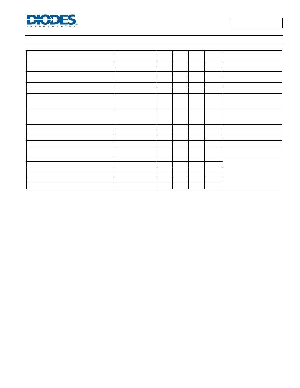
Electrical Characteristics - Q1 & Q2 common
(@T
A
= +25°C, unless otherwise specified.)
Characteristic Symbol
Min
Typ
Max
Unit
Test
Condition
Collector-Base Breakdown Voltage
BV
CBO
80
V
I
C
= 100µA
Collector-Emitter Breakdown Voltage (Note 13)
BV
CEO
60
V
I
C
= 10mA
Emitter-Base Breakdown Voltage
BV
EBO
5
V
I
E
= 100µA
Collector-Base Cutoff Current
I
CBO
100 nA
V
CB
= 60V, I
E
= 0A
50 µA
V
CB
= 60V, I
E
= 0A, T
J
= +150°C
Collector-Emitter Cutoff Current
I
CES
100 nA
V
CES
= 60V, V
BE
= 0V
Emitter-Base Cutoff Current
I
EBO
100 nA
V
EB
= 5V, I
C
= 0A
DC Current Gain (Note 13)
h
FE
250
200
100
380
420
380
I
C
= 1mA, V
CE
= 5V
I
C
= 500mA, V
CE
= 5V
I
C
= 1A, V
CE
= 5V
Collector-Emitter Saturation Voltage (Note 13)
V
CE(sat)
60
70
100
110
140
250
mV
I
C
= 100mA, I
B
= 1mA
I
C
= 500mA, I
B
= 50mA
I
C
= 1A, I
B
= 100mA
Equivalent On-Resistance
R
CE(sat)
100 250 mΩ
I
C
= 1A, I
B
= 100mA
Base-Emitter Saturation Voltage (Note 13)
V
BE(sat)
940 1100 mV I
C
= 1A, I
B
= 50mA
Base-Emitter Turn-On Voltage (Note 13)
V
BE(on)
780 900 mV
I
C
= 1A, V
CE
= 5V
Output Capacitance
C
obo
5.5 10 pF
V
CB
= 10V, f = 1MHz
Transition Frequency
f
T
150 220
MHz
V
CE
= 10V, I
C
= 50mA
f = 100MHz
Turn-On Time
t
on
63
ns
V
CC
= 10V, I
C
= 0.5A
I
B1
= -I
B2
= 25mA
Delay Time
t
d
33
ns
Rise Time
t
r
30
ns
Turn-Off Time
t
off
420
ns
Storage Time
t
s
380
ns
Fall Time
t
f
40
ns
Notes:
13. Measured under pulsed conditions. Pulse width ≤ 300 µs. Duty cycle ≤ 2%