Safe operating area, Derating curve, Transient thermal impedance – Diodes DSS4160DS User Manual
Page 3: Pulse power dissipation, Dss4160ds, Thermal characteristics and derating information, Coll ec tor curr en t ( a ) v, Collector-emitter voltage (v), Therm al r es ist an ce ( °c/ w) pulse width (s), Pulse width (s) t herm al resi st ance ( °c/ w)
DSS4160DS
Document number DS36556 Rev. 1 – 2
3 of 7
November 2013
© Diodes Incorporated
DSS4160DS
Thermal Characteristics and Derating Information
100µ
1m
10m 100m
1
10
100
1k
0
20
40
60
80
100
120
140
100m
1
10
10m
100m
1
T
amb
=25°C
25mm x 25mm
1oz FR4
V
CE(sat)
Limit
100µs
1ms
10ms
100ms
1s
DC
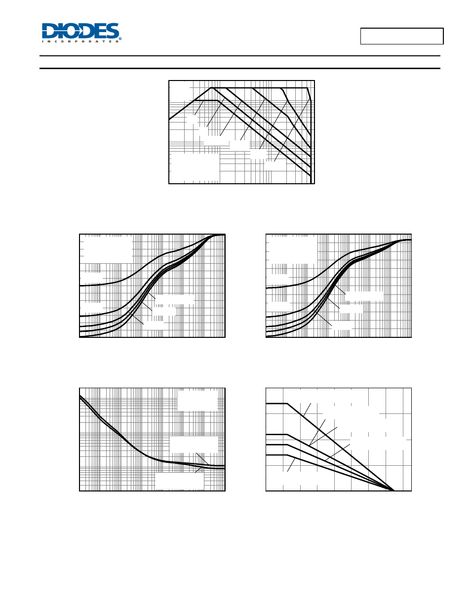
Safe Operating Area
I
C
C
oll
ec
tor Curr
en
t (
A
)
V
CE
Collector-Emitter Voltage (V)
0
20
40
60
80 100 120 140 160
0.0
0.5
1.0
1.5
2.0
15mm x 15mm 1oz FR4
one active die
50mm x 50mm 2oz FR4
One active die
25mm x 25mm 1oz FR4
one active die
25mm x 25mm 1oz FR4
Two active die
50mm x 50mm 2oz FR4
One active die t<5secs
Derating Curve
Temperature (°C)
M
a
x P
ower Di
ss
ip
at
io
n (W)
100µ
1m
10m 100m
1
10
100
1k
0
20
40
60
80
100
120
T
amb
=25°C
25mm x 25mm
1oz FR4
Transient Thermal Impedance
D=0.5
D=0.2
D=0.1
Single Pulse
D=0.05
T
herm
al
R
es
ist
an
ce (
°C/
W)
Pulse Width (s)
100µ
1m
10m 100m
1
10
100
1k
1
10
100
25mm x 25mm
1oz FR4
50mm x 50mm
2oz FR4
Single Pulse
T
amb
=25°C
Pulse Power Dissipation
Pulse Width (s)
M
a
x P
ower Di
ss
ip
at
io
n (W)
D=0.1
D=0.05
Single Pulse
D=0.2
D=0.5
T
amb
=25°C
50mm x 50mm
2oz FR4
Transient Thermal Impedance
Pulse Width (s)
T
herm
al
Resi
st
ance (
°C/
W)