Preliminary datasheet, Parameter symbol condition value unit – Diodes AZ4052 User Manual
Page 5
Preliminary Datasheet
Dual 4-channel Analog Multiplexer/Demultiplexer AZ4052
Oct. 2011 Rev. 1. 1 BCD Semiconductor Manufacturing Limited
5
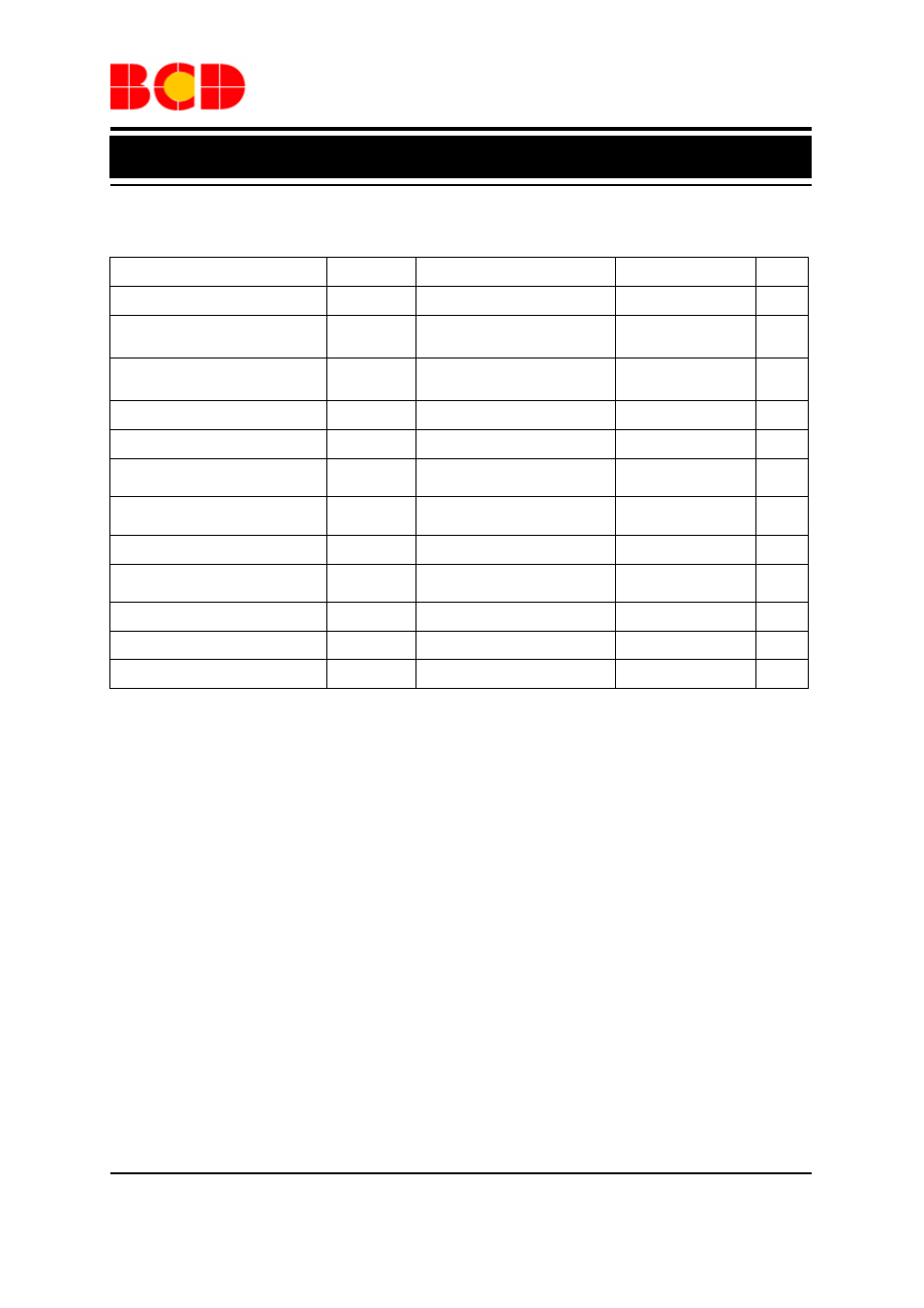
Absolute Maximum Ratings (Note 1, 2)
Parameter
Symbol Condition
Value
Unit
Power Supply Voltage
V
CC
-0.5 to 11.0
V
Input Diode Current
I
IK
V
I
<
-0.5V,
V
I
>
V
CC
+0.5V
20 mA
Switch Diode Current
I
SK
V
S
<
-0.5V,
V
S
>
V
CC
+0.5V
20 mA
Switch Current
I
S
-0.5V<V
S
<
V
CC
+0.5V 25 mA
V
EE
Current I
EE
20
mA
V
CC
Current
GND Current
I
CC
I
GND
50
mA
Power Dissipation
P
D
T
A
=-40ºC to 85ºC
(Note 3)
500 mW
Storage Temperature Range
T
STG
-65
to
150
ºC
Operating Junction
Temperature Range
T
J
150
ºC
Power Dissipation Per Switch
P
S
100
mW
ESD (Machine Model)
200
V
ESD (Human Body Model)
2000
V
Note 1: Stresses greater than those listed under “Absolute Maximum Ratings” may cause permanent damage to
the device. These are stress ratings only and functional operation of the device at these or any other conditions
beyond those indicated under “Recommended Operating Conditions” is not implied. Exposure to “Absolute
Maximum Ratings” for extended periods may affect device reliability.
Note 2: To avoid drawing V
CC
current out of pins nZ, when switch current flows in pins nYn, the voltage drop
across the bidirectional switch must not exceed 0.4V. If the switch current flows into pins nZ, no VCC current
will flow out of pins nYn. In this case there is no limit for the voltage drop across the switch, but the voltages at
pins nYn and nZ may not exceed V
CC
or V
EE
.
Note 3: Above 70ºC derate linearly with 12mW/K (DIP-16 package).
Above 70ºC derate linearly with 8mW/K (SOIC-16 package)