Data sheet, Pin description (continued) – Diodes CS5519 User Manual
Page 5
Data Sheet
Enhanced Multi-touch Capacitive Touch Screen Controller CS5519
Apr. 2013 Rev. 1. 0 BCD Semiconductor Manufacturing Limited
5
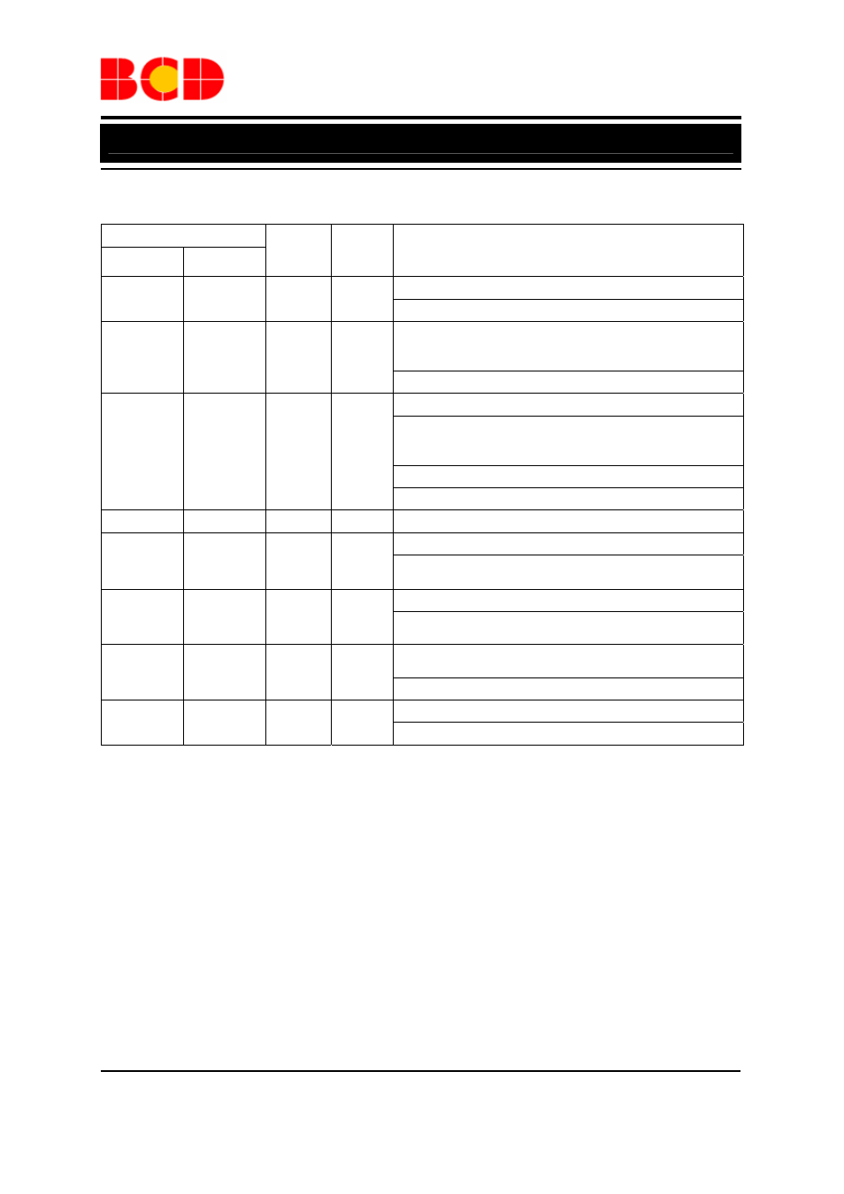
Pin Description (Continued)
Pin Number
Pin
Name
Pin
Type
Pin Function
QFN-7×7
-56
QFN-8×8
-68
-
6 to 13
D38 to
D31
O, A
D38, D37, D36, D35, D34, D33, D32, D31
Driving line 38 to line 31
6 to 35
14 to 43
D30 to
D1
O, A
D30, D29, D28, D27, D26, D25, D24, D23, D22, D21,
D20, D19, D18, D17, D16, D15, D14, D13, D12, D11,
D10, D9, D8, D7, D6, D5, D4, D3, D2, D1
Driving line 30 to line 1
36 44
P3.6/
RXD1
(open-
drain)
I/O
Port 3.6 GPIO
8051 P3.6 GPIO
This pin should be configured as open-drain output and
the input range can be 1.8V to 3.3V
RXD1
This pin also can be configured as RXD of UART 1
37 69
VSS
Power
Ground Voltage. 0V
38 45
VDD18
Power
Internal Regulator Output. 1.6V to 2.0V
Typical decoupling capacitors of 0.1
F and 10F should
be connected between VDD18 and VSS
39 46
VDD33
Power
Supply Voltage. 2.8V to 3.6V
A good decoupling capacitor between VDD33 and VSS is
critical for good performance
40 to 56
47 to 63
S1 to
S17
I, A
S1, S2, S3, S4, S5, S6, S7, S8, S9, S10, S11, S12, S13,
S14, S15, S16, S17
Sensing line 1to line 17
- 64
to
68
S18 to
S22
I, A
S18, S19, S20, S21, S22
Sensing line 18 to line 22