Ap8802, 1a led step-down converter, Pin descriptions – Diodes AP8802 User Manual
Page 2: Functional block diagram
AP8802
1A LED STEP-DOWN CONVERTER
AP8802
Document number: DS31766 Rev. 9 - 2
2 of 19
www.diodes.com
May 2012
© Diodes Incorporated
Pin Descriptions
Name
SO-8
SO-8EP
U-DFN3030-10
Function
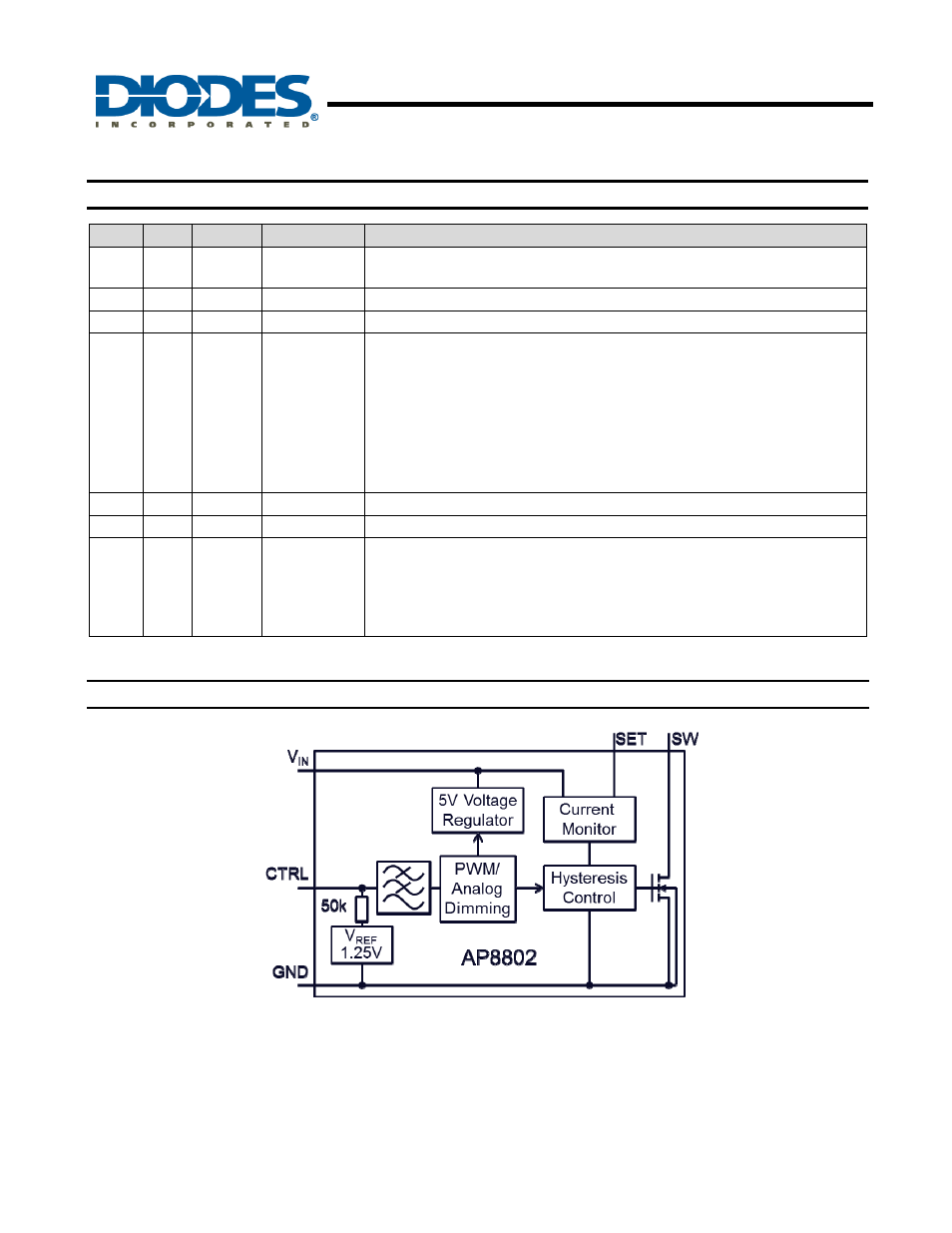
SW
6, 5
6, 5
7, 6
Switch Pin. Connect inductor/freewheeling diode here, minimizing track length at this pin
to reduce EMI.
GND
2
2
2, 9
GND pin
SET
1
1
1
Set Nominal Output Current Pin. Configure the output current of the device.
CTRL 8
8
10
Dual function dimming control pin.
• Input voltage of 0.2V or lower forces the device into low current standby mode
and shuts off the output.
• A PWM signal (driven by an open-drain/collector source) allows the output
current to be adjusted over a wide range up to 100%.
• An analog voltage between 0.3V and 2.5V adjusts the output current between
25% and 200% of the current set by 0.2V/R
S
.
The input impedance is about 50k
Ω, and if the pin is left open V
CTRL
= V
REF
V
IN
4
4
5
Input Supply Pin. Must be locally bypassed.
NC
3
3
3, 4, 8
No connection
EP - EP
EP
Exposed pad: Internally connected to IC substrate.
It should be connected to GND and as large as possible thermal mass for improved
thermal impedance and power dissipation capability.
However the exposed pad is not a Power GND return path. The dedicated GND pins must
be connected to 0V. See Land Pad diagrams.
Functional Block Diagram
Figure. 1 Functional Block Diagram